Reports 1-1 of 1 Clear search Modify search
IOO (General)
takafumi.ushiba - 18:00 Monday 22 December 2025 (35926) Print this report
Optical gain measurement of PMC

[Tanaka, Ushiba]

Abstract:

PMC optical gain was measured by sweeping laser frequency.
Measured optical gain is 1.15e-5 V/Hz at K1:PSL-PMC_MIXER_MON_OUT_DQ.

Detail:

For the PMC characterization, we tired to measure PMC optical gain by sweeping the laser frequency.
Measurement procedure is as follows:
1. Unlock PMC by requesting the DOWN state to the IO guardian.
2. Open RAMP switch of PMC TTFSS servo (K1:PSL-PMC_RAMP_ON) to avoid sensing feedback signals to PZT.
3. Close the input switch of PMC TTFSS servo (K1:PSL-PMC_TEST1_ON) to send the PDH signals to MIXER OUT DAQ.
4. Change TEMP bias for NPRO laser (K1:IMC-SERVO_NPRO_TEMP_BIAS_OFFSET) by 0.02 (In our case, 0.32 to 0.3) with 120 sec ramptime.
5. Calculate the sweep speed from FSR.
6. Calculate the slope of PDH signals from PDH signals when PMC was resonated with TEM00.

Figure 1 shows the PMC error signals, TEMP bias offset in the unit of  DAC cnts, and PMC transmission power during the sweep.
According to the time difference between two resonances (19.52 s), sweep speed can be estimated as 7.60 MHz/s (148.4/19.52).
Note that 148.4 in the calculation is PMC FSR, which is calculated by speed of light and PMC round trip length (2.02 m).

Figure 2 shows the enlarged view fo figure 1 around the resonance.
The slope of PMC error signals is 87.16 V/s (87.16 mV with 1 ms).
So, the optical gain measured at K1:PSL-PMC_MIXER_MON_OUT_DQ is 1.15e-5 V/Hz.

Discussion:

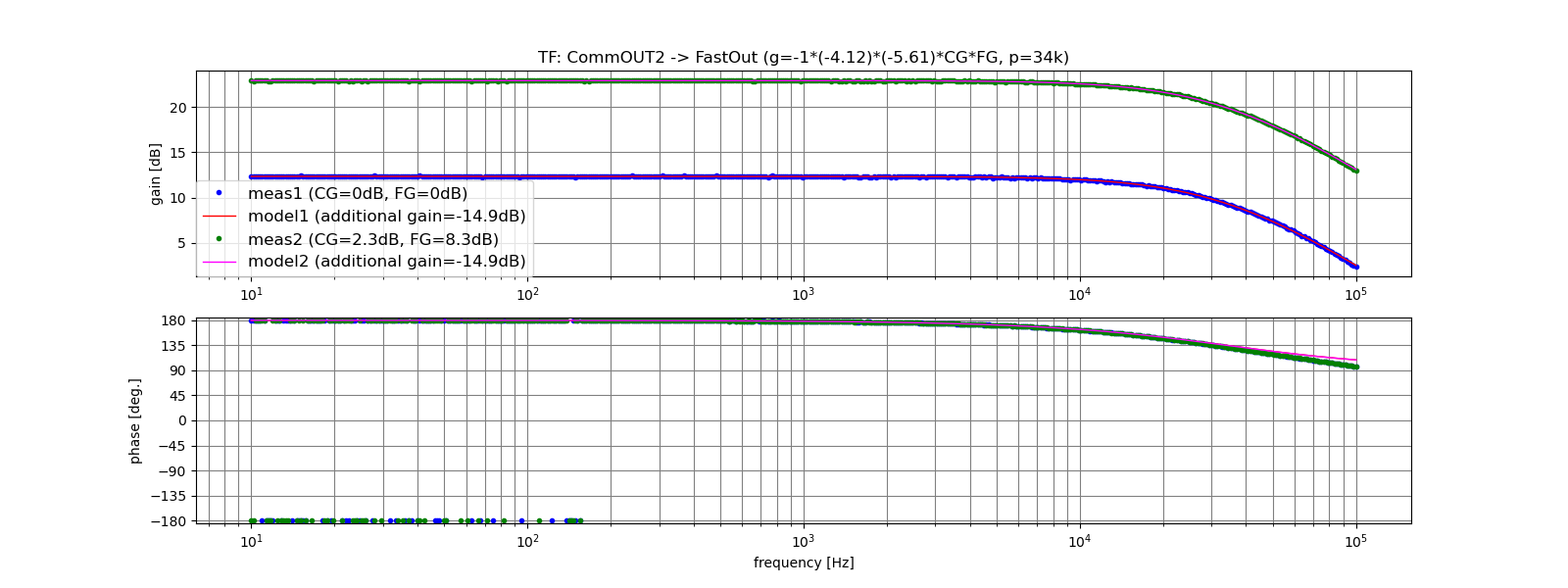
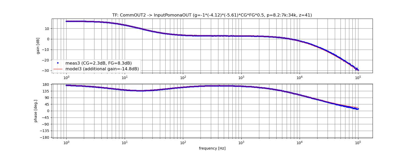
The previous optical gain measurement is reported in klog16367, which is estimated by OLTF and the other transfer functions.
The current COMMON and FAST gain values are 2.3 dB and 8.3 dB while they are 21.2 dB and 17.2 dB (fig3), respectively.
So, the optical gain should be increased by 27.8 dB campared to the previous measurement.
In addition, the previous measurement calculated the optical gain at just after the mixer inside TTFSS but the value calculated this time is that at K1:PSL-PMC_MIXER_MON_OUT_DQ.
Since there is a gain of 3 between mixer output and K1:PSL-PMC_MIXER_MON_OUT_DQ, so the optical gain should be increased by a factor of 3.16 (~10dB).
So, the gain should be increased by 37.8 dB from the previous value.

The difference between the values measured this time and previous time is 9.8 dB.
Note that we are not so sure this difference is reasonable or not because the laser source and EOM were different from the previous measurement and PMC OLTF is not measured yet with the current configuation.

Images attached to this report
Comments to this report:
takafumi.ushiba - 20:33 Tuesday 23 December 2025 (35934) Print this report

[Yamamoto, Ushiba]

We compared the measured OLTF reported in klog35931 with the OLTF model calculated from circuits (klog5399), actuator efficiency (klog35875), and optical gains reported in the original post.
Figure 1 shows the results and the gain of OLTF model seems too high, so there seems some mistakes or misunderstandings in the model calculation.

Figure 2 shows the block diagram of the PMC loop.
C_PMC is cavity pole of the PMC with time delay, which was measured as 610kHz with 1.17 us (klog7218).
S_PMC is a optical gain of PMC, which was measured as 3.64e-6 V/Hz (1.15e-5/3.16). Note that the measured value in the original post includes the gain of G_0 in the diagram, which is the gain between mixer output and pick off port of error signals, and the value is 3.16 according to the electrical circuit diagram (JGW-D1301823-v2).
G_C and G_F are the common and fast gains, which are recently 2.3 and 8.3 dB, respectively.
F_T is the filter of TTFSS and overall gain of 4.12*5.61 with notch filters around several hundred kHz according to the modification summary (klog5399).
F_pin is the filter of pomodo box installed at the input of high voltage amplifier (klog5372).
G_HV and G_mon are gains of high voltage amplifier (32.88 according to klog5396) and its monitor port, respectively.
A_PZT is an actuator efficiency of PZT including the frequency response due to the output pomodo box installed just after the HV output (klog5372).

Since there seems no log on the TF measurement of circuit itself, it would be better to check the TF of the circuit (from G_0 to F_pin , G_HV, and A_PZT).
Today, to measure the frequency response of A_PZT, I measured the TF from v_mon to v_error with PMC lock (fig3), which is almost consistent with the value reported in klog5372.
Note that HV_OUT_DQ including the 37Hz pole foton filter, so low-pass filter trend is canceled out.
The other part of TF measurement should be done inside the mine later.

Images attached to this comment
takahiro.yamamoto - 14:08 Wednesday 24 December 2025 (35942) Print this report

Memo about the gain stages of TTFSS.

Common gain and Fast gain are implemented by AD602J.
According to the data sheet, the relation between the input voltage and available gain in the unit of dB is
dB = 32 * V + 10
<=> V = (dB - 10) / 32


This conversion factor is implemented in the FilterBank (K1:PSL-PMC_{COMMON,FAST}_GAIN_CALI) as shown in Fig.1.
gain(3276.8) is a factor of ct/V and gain(0.3185) probably consists from a factor of 1/32 (dB->V) and a factor of 10 (compensation of 0.1 gain at TTFSS Interface board).
So dB values shown on MEDM represents a gain between the input and the output of AD602J.

On the other hand, actual implementation is to add resistance at the input of AD602J without opamp as shown in Fig.2 (see also JGW-D1301823) and voltage drop at this resistance doesn't seem to be negligible.
According to the spice simulation, available gain with 0V as input voltage are 4.5dB and 2.6dB for common gain and fast gain as shown in Fig.3 though 10dB are shown on MEDM in the case of 0V input.
A part of mismatch between the model and measurements may comes from these differences (5.5dB for common gain and 7.4dB for fast gain).

Spice model used in this check is available in /users/AEL/LTspice/asc/TTFSS_JGW-D1301751/

Images attached to this comment
takafumi.ushiba - 23:58 Wednesday 24 December 2025 (35945) Print this report

I measured following transfer function (All TF measurement were done by injecting signals from TEST of TTFSS RF circuit).
1. TEST to common OUT1 and  common OUT2,  and common OUT1 to common OUT2.
2. Common OUT2 to FAST out with common gain of 0 dB and FAST gain of 0 dB on the medm screen.
3. Common OUT2 to FAST out with common gain of 2.3 dB and FAST gain of 8.3 dB on the medm screen.
4. Common OUT2 to Pomona box out connected to HV amp input  with splitting to BNC-T (fig1). the gain setting for the measurement is same as 3.

All data are stored on kagra dropbox (Apps/Liquid Instruments/) with the file name starting from "TF_TTFSS".
Detail will besummarized after finishing comparison between theory and measured data.

Images attached to this comment
takahiro.yamamoto - 2:44 Thursday 25 December 2025 (35949) Print this report

According to the comparison plots of 4 measurements and corresponding models, respectively, there should be unknown gain as -14.9dB~-14.8dB which seems to be an effect of the resistance at the input of AD602J as reported in klog#35942.

1) From RF_TEST to Common_OUT2
This TF contains notch at MHz band (L3 and C12-14 of TTFSS RF board) and the inverting amplifier circuit (U3 of TTFSS main board). Design value of the gain is 10.00dB. Measured TF shows ~9.65dB (Fig.1) and it's reasonable if resistances has ~3-5% variability.

2), 3) From Common_OUT2 to FAST_OUT with two cases of Common Gain (CG) and Fast Gain (FG) settings
This TF contains CG, FG, U9 (gain=-4.12, pole=34kHz), U7 (gain=-5.61), U11 (gain=-1.0) and U10 (gain=1.0) of TTFSS main board (U8 was omitted according to klog#306). As reported in klog#35945, measurement was done with two cases of (CG, FG) settings as (0dB, 0dB) and (2.3dB, 8.3dB). These models for two cases have -14.8dB mismatch from measured values (Fig.2). This fact seems to support an effect of the resistance at the input of AD602J (roughly -13dB) reported in klog#35942.

4) From Common_OUT2 to Pomona Output
This TF contains same components as 2), 3) and Pomona box (gain=-6dB, pole=8.2Hz:7kHz, zero=41Hz). A gain of Pomona box as -6dB comes from output load of the Pomona box and input impedance of HV amp as shown in Fig.3. CG and FG during this measurement were 2.3dB and 8.3dB, respectively (see again klog#35945). A mismatch between the model and measured TF as a factor of -14.8dB can be seen also for this TF as shown in Fig.4.

Images attached to this comment
takafumi.ushiba - 13:43 Thursday 25 December 2025 (35954) Print this report

I mde overplots of each measured transfer function with models.

Figure 1 shows the TF from TTFSS:RF TEST to TTFSS:Common Path OUT1.
The gain of this part seems well matched with the theoretical estimation.

Figure 2 shows the TF from TTFSS:Common Path OUT1 to TTFSS:Common Path OUT2.
According to the circuit diagram, the gain of this part should be -3.16 (392/124) but the measured value is slightly lower than expectation.
So, I made an adjusted TF model that has a gain of -2.944, which seems to match with the measured values well.

Figure 3 shows the TF from TTFSS:Common Path OUT2 to TTFSS:PZT Path FAST OUT with Common and FAST gains of 0 dB.
In this part, we have U2A, U2B, U9, U7, U11, and U10, which have a gain of -5.5dB (klog35942), -7.3dB(klog35942) , -4.12 (3090/750), -5.61 (5600/998), -1 (5600/5600), and 1, respectively.
In addition, U9 has a pole at 34.3 kHz.
Note that U8 was removed according to klog3599.
Since there is a gain of 0.778 difference between measured values and theoretical mode, I adjuted the model gain by adding the gain of 0.778 as shown in the fig3 (model (adjusted)).

Figure 4 shows the same measurment with different common (2.3 dB) and fast (8.3 dB) gains on the medm screen.
Since the difference between the model (theory) and measured values are same as fig3, relatve gain change on the medm seems to work well.

Figure 5 shows the TF from TTFSS:Common Path OUT2 to Pomona box OUT, which is installed just before the high-voltage amplifier input (klog5372).
Since this pomona box behaviour is changed when disconnecting from the HV amplifier, I connected the Moku:Lab by pick up the signals with BNC-T as shown in fig6.
In this part, there should be an additional gain of 0.5, poles of 8.4 Hz and 7 kHz, and a zero of 41 Hz.
According to the comparison with the model and measured data, the theoretical TF of this part seems to work well.

Figure 7 shows the OLTF model based on the above adjusted circuit TF models, optical efficiency measured in the original post, and actuator efficiency.
Though the difference becomes smaller owing to the changes of the gains of circuit in the models, there is still one order of magnitude difference between measured OLTF and OLTF model.

Images attached to this comment
takafumi.ushiba - 22:29 Thursday 25 December 2025 (35960) Print this report

Abstract:

I tried cavity scan again and obtained the optical gain as (1.6 +/- 1.1)e-6 V/Hz.
In addition, I calculated the optical gain from the fitting of OLTF and obtained 8.5e-7 V/Hz, which is consistent with the value measured by cavity scan.

Detail:

I remeasured the optical gain of PMC with 10 times higher scan speed (I changed K1:IMC-SERVO_NPRO_TEMP_BIAS_OFFSET by 0.2 with 60 seconds ramptime).
In addition, I used the peak around the center of the scan time to use the data when the scan speed is stable as much as possible.
Furthermore, I calculated the optical gain by using both forward and backwrd scan data to evaluate the systematic error.

Figure 1 shows the data during forward scan.
I used two peaks overlapped with T cursors to calculate the scan speed and the peak between T cursor to calculate the slope of PDH signals.
According to fig1, 2FSR is corresponding to 3.903 seconds, so the scan speed is 7.61e7 Hz/s.
Figure 2 shows the enlarged view of the peak between the T cursors in fig1.
The slope of the PDH signals are 203.3 V/s, so the optical gain can be estimated as 2.67e-6 V/Hz.

Figure 3 and 4 show the similar ndscope screem in fig1 and fig2 during backward scan.
The scan speed and slope of PDH signals are 7.60e7 Hz/V and 42.96 V/s, which is corresponding to the optical gain of 5.65e-7 V/Hz.

Since the optical gain of PMC should be between these two values, the optical gain can be estimated as (1.6 +/- 1.1)e-6 V/Hz.
I also calculated the optical gain from the fitting of the measured OLTF between 500 Hz to 10 kHz and obtained 0.85e-6 V/Hz, which is consistent with the above measurement.
Figure 5 shows the overplot of measured OLTF and OLTF model with the optical gain of 0.85e-6 V/Hz.

Note:

The main problem of the cavity scan measurement is thermal expansion of PMC, which causes large difference between forward and backward measurement, so the effect can be mitigated if we measure with low power.
Since TF of electrical circuit and PZT actuator should not be changed, we would evaluate the PMC optical gain from the OLTF measurement if we will once characterize them with low power.

Images attached to this comment
Search Help
×

Warning

×