Memo about the gain stages of TTFSS.
Common gain and Fast gain are implemented by AD602J.
According to the data sheet, the relation between the input voltage and available gain in the unit of dB is
dB = 32 * V + 10
<=> V = (dB - 10) / 32
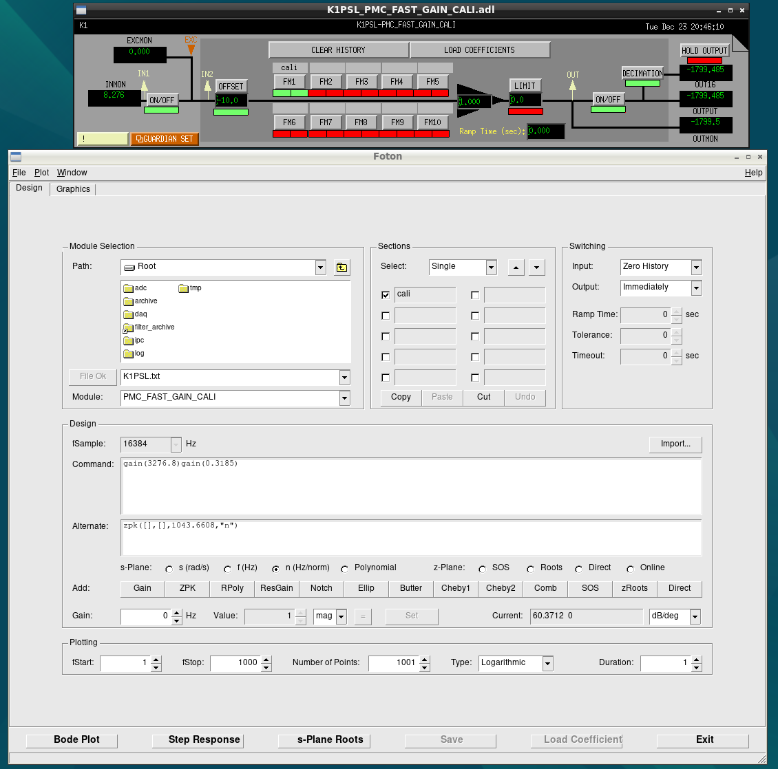
This conversion factor is implemented in the FilterBank (K1:PSL-PMC_{COMMON,FAST}_GAIN_CALI) as shown in Fig.1.
gain(3276.8) is a factor of ct/V and gain(0.3185) probably consists from a factor of 1/32 (dB->V) and a factor of 10 (compensation of 0.1 gain at TTFSS Interface board).
So dB values shown on MEDM represents a gain between the input and the output of AD602J.
On the other hand, actual implementation is to add resistance at the input of AD602J without opamp as shown in Fig.2 (see also JGW-D1301823) and voltage drop at this resistance doesn't seem to be negligible.
According to the spice simulation, available gain with 0V as input voltage are 4.5dB and 2.6dB for common gain and fast gain as shown in Fig.3 though 10dB are shown on MEDM in the case of 0V input.
A part of mismatch between the model and measurements may comes from these differences (5.5dB for common gain and 7.4dB for fast gain).
Spice model used in this check is available in /users/AEL/LTspice/asc/TTFSS_JGW-D1301751/


