According to the comparison plots of 4 measurements and corresponding models, respectively, there should be unknown gain as -14.9dB~-14.8dB which seems to be an effect of the resistance at the input of AD602J as reported in klog#35942.
1) From RF_TEST to Common_OUT2
This TF contains notch at MHz band (L3 and C12-14 of TTFSS RF board) and the inverting amplifier circuit (U3 of TTFSS main board). Design value of the gain is 10.00dB. Measured TF shows ~9.65dB (Fig.1) and it's reasonable if resistances has ~3-5% variability.
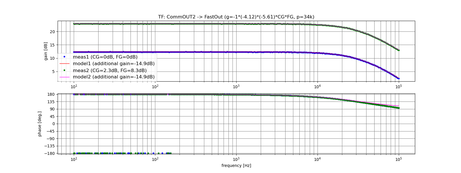
2), 3) From Common_OUT2 to FAST_OUT with two cases of Common Gain (CG) and Fast Gain (FG) settings
This TF contains CG, FG, U9 (gain=-4.12, pole=34kHz), U7 (gain=-5.61), U11 (gain=-1.0) and U10 (gain=1.0) of TTFSS main board (U8 was omitted according to klog#306). As reported in klog#35945, measurement was done with two cases of (CG, FG) settings as (0dB, 0dB) and (2.3dB, 8.3dB). These models for two cases have -14.8dB mismatch from measured values (Fig.2). This fact seems to support an effect of the resistance at the input of AD602J (roughly -13dB) reported in klog#35942.
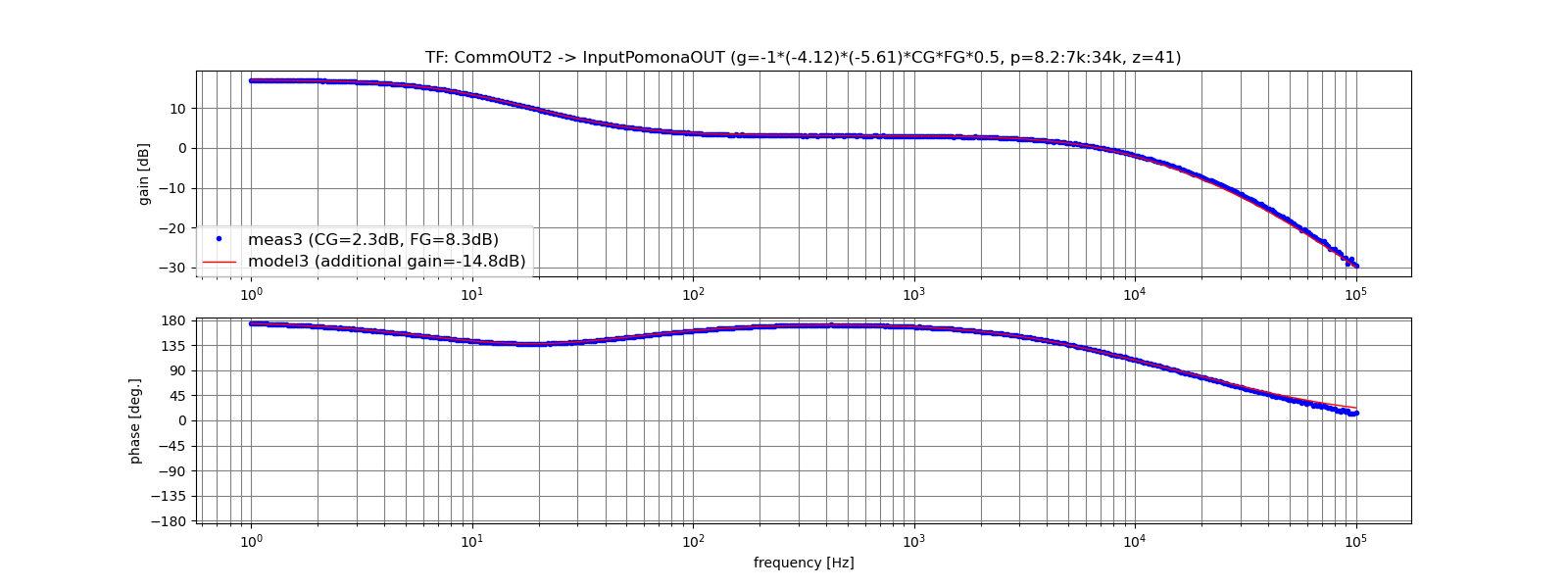
4) From Common_OUT2 to Pomona Output
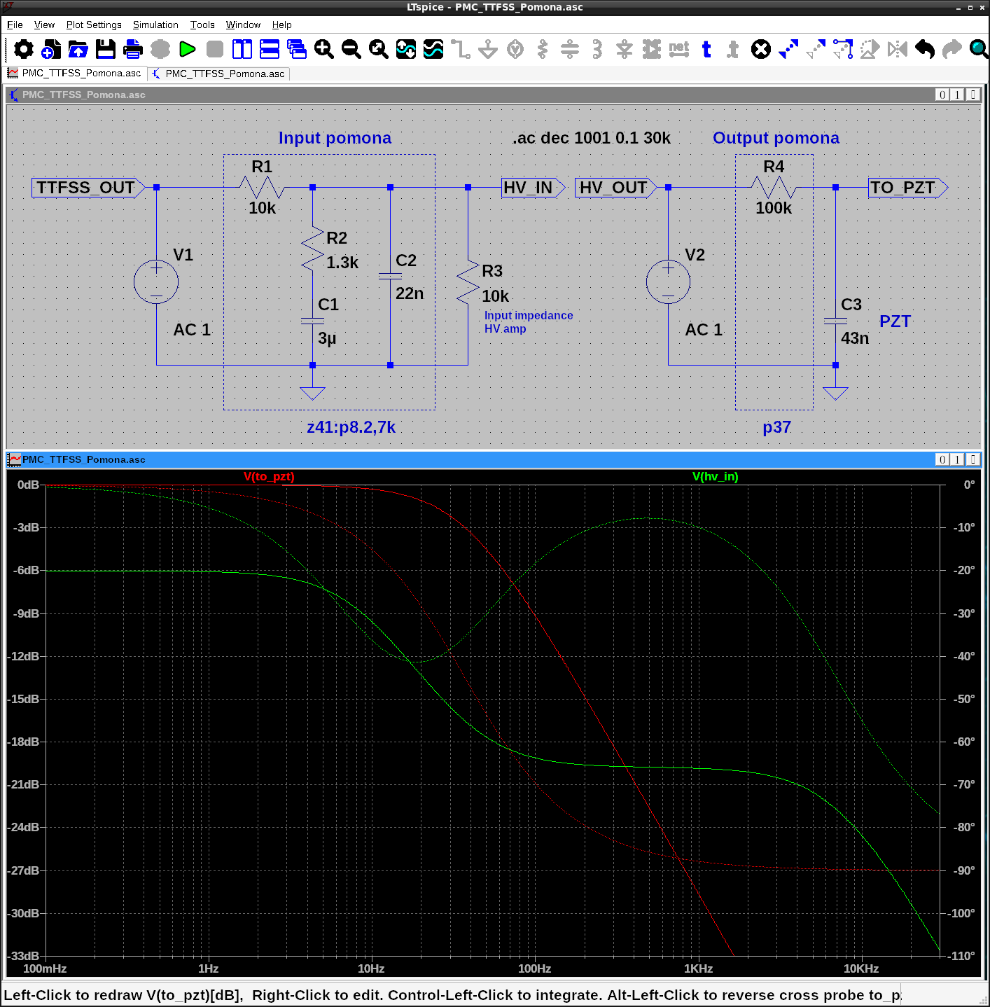
This TF contains same components as 2), 3) and Pomona box (gain=-6dB, pole=8.2Hz:7kHz, zero=41Hz). A gain of Pomona box as -6dB comes from output load of the Pomona box and input impedance of HV amp as shown in Fig.3. CG and FG during this measurement were 2.3dB and 8.3dB, respectively (see again klog#35945). A mismatch between the model and measured TF as a factor of -14.8dB can be seen also for this TF as shown in Fig.4.


