YamaT, Uchiyama, Akutsu
Abstract
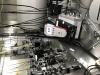
PMC stable lock has been mostly recovered (Fig. 11). Still some concerns in the thermal control path.
Details
As reported in 16222, after the sudden blackout on the last Friday (Mar. 5), the Dsub-to-BNC converter (S1605873) in the PSL room did not work well (at least for the shutter), and so we determined to use it by closing the jumper pins in the converter so that we were sure to obtain the signal outputs.
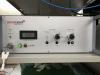
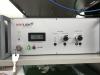
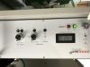
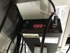
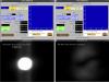
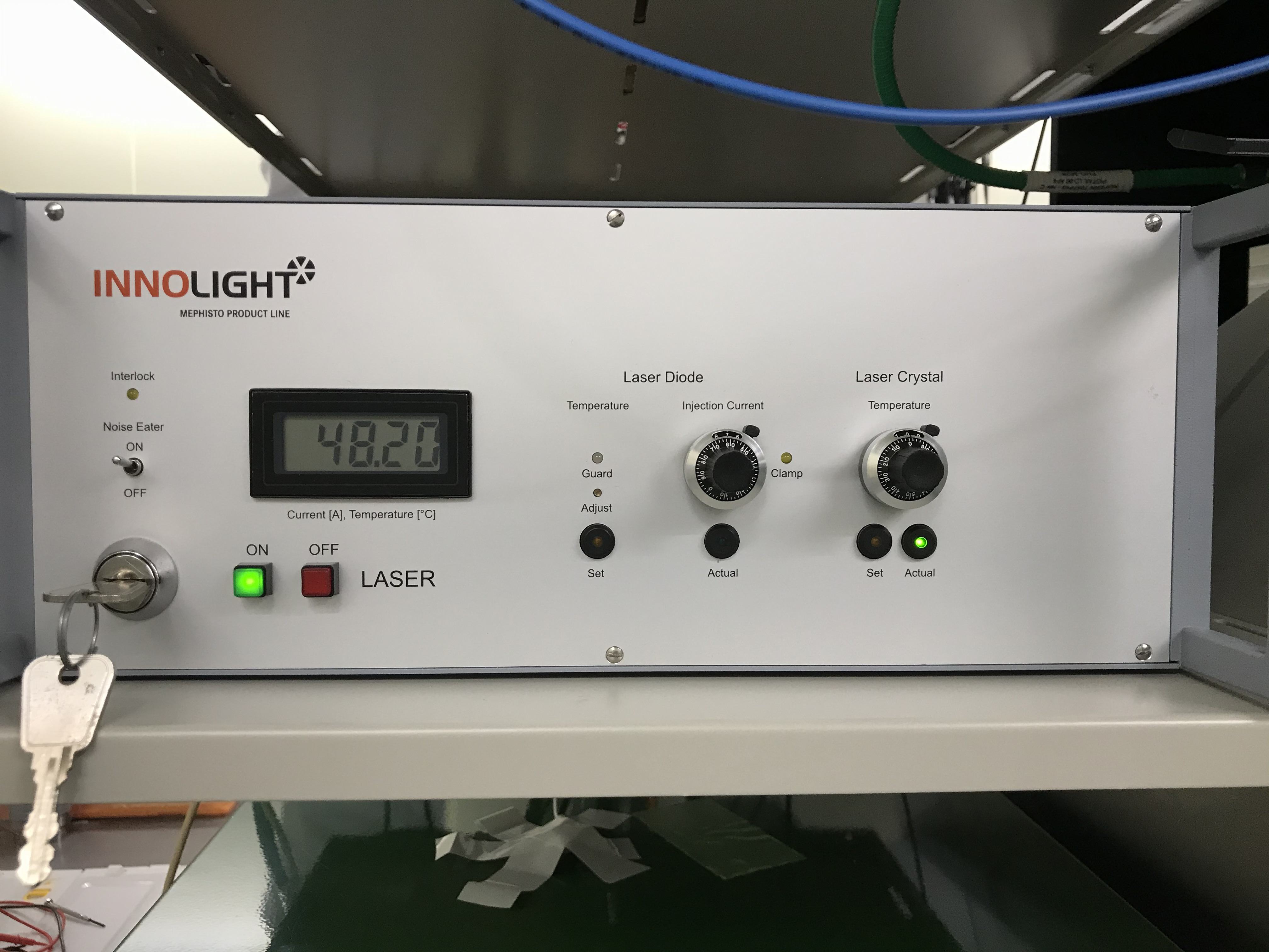
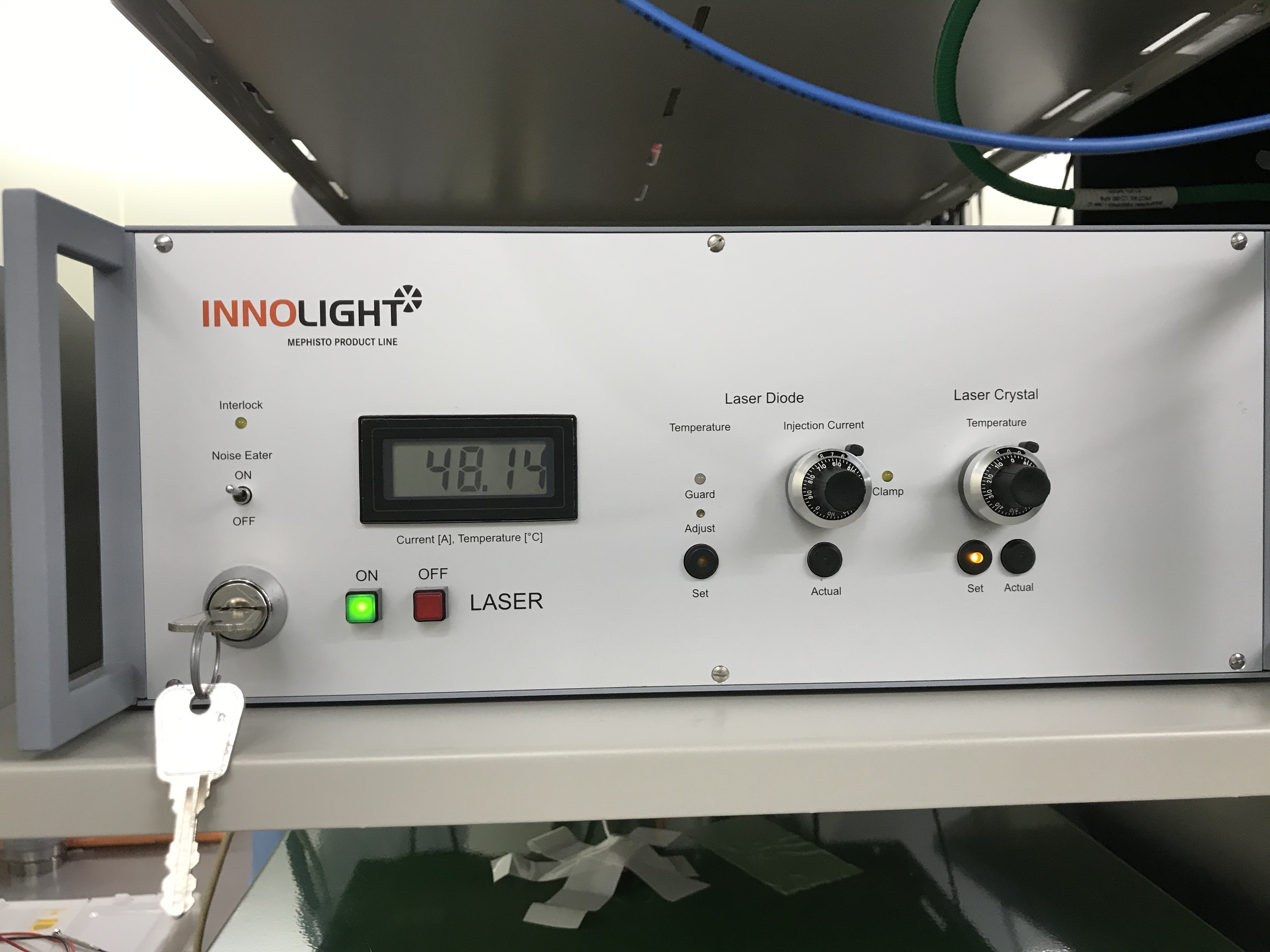
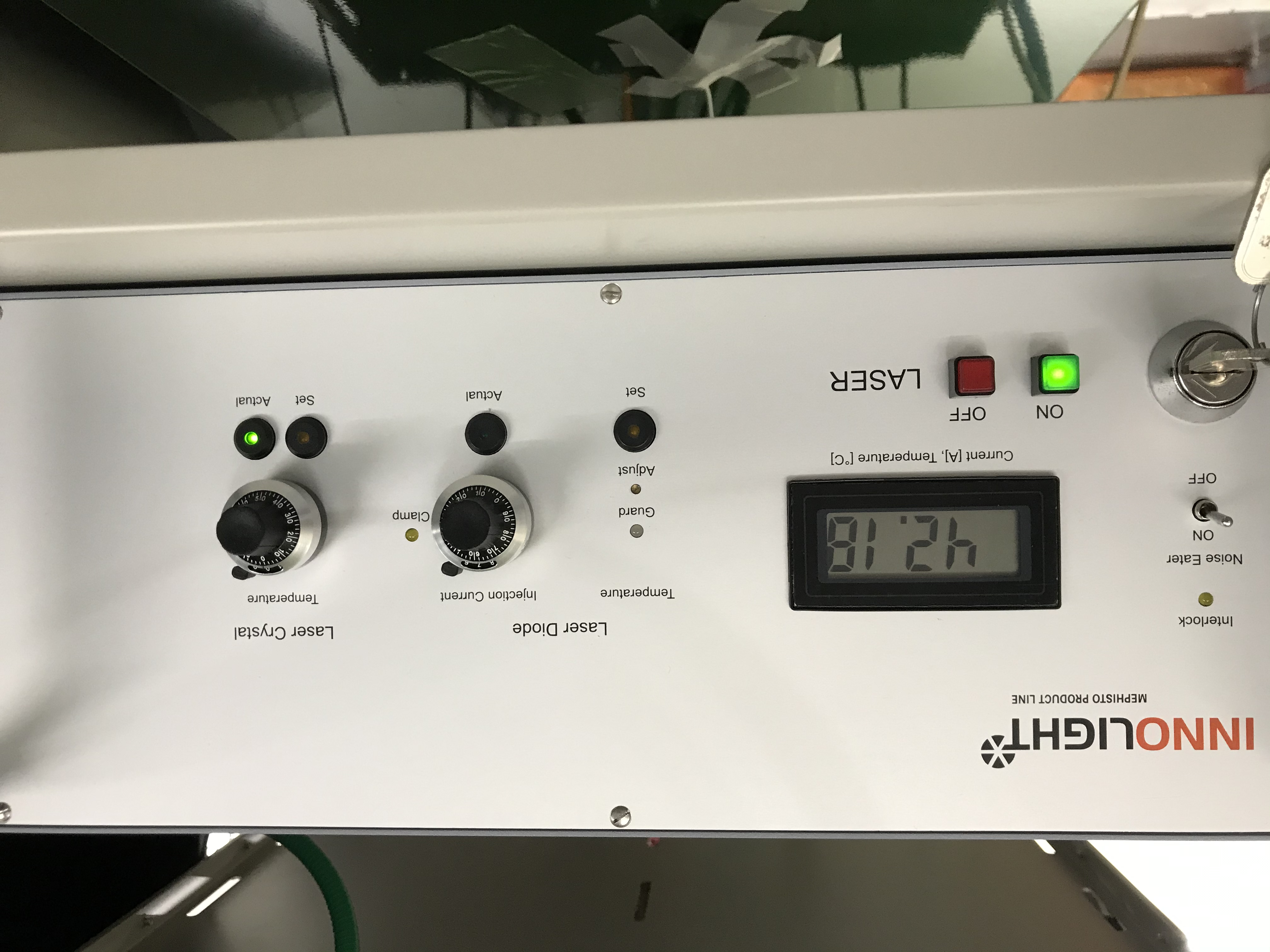
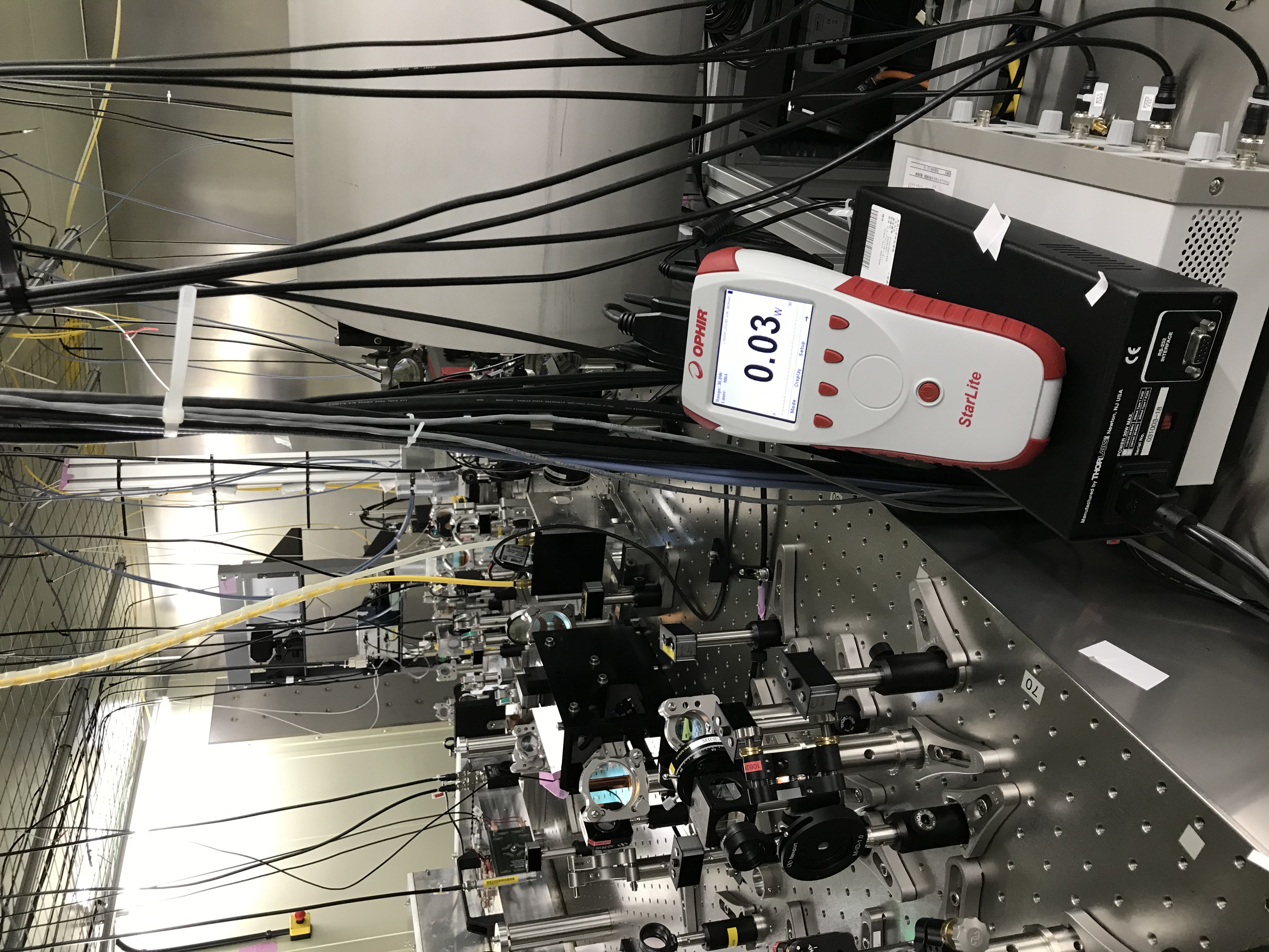
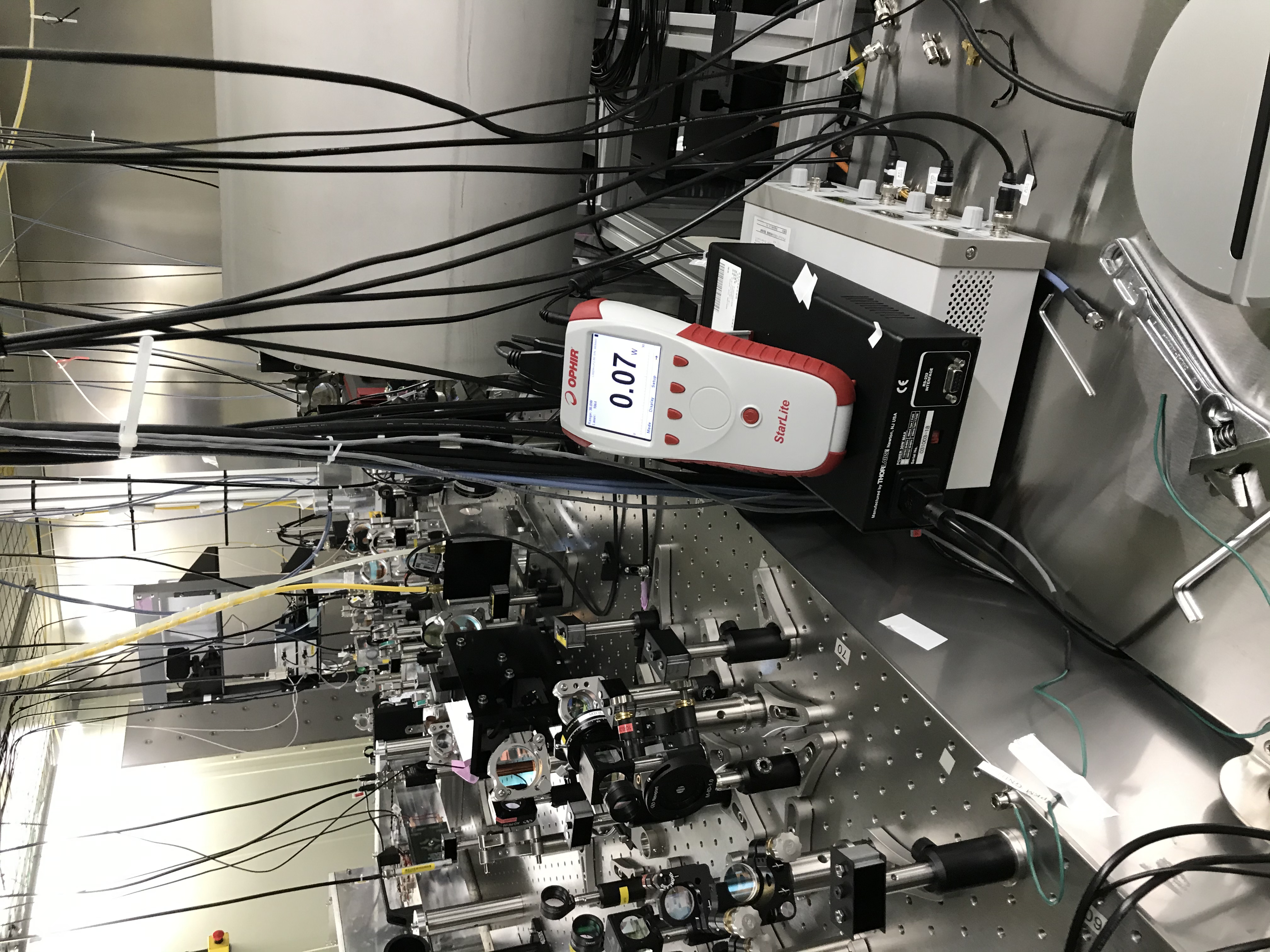
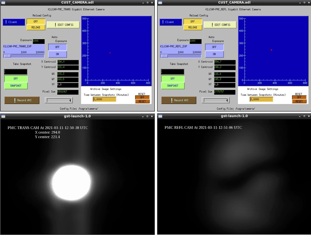
- Ch.16: provides a bias voltage to the seed laser (Innolight); the laser crystal temperature in the display changed from 48.20 deg ("set" has been 48.14 deg) to 42.18 deg (Figs. 1, 2, and 3, respectively), so the bias lowered the laser crystal temperature about 6 deg. Then, when we locked the PMC, the behavior seemed recovered to that on Mar. 9; the input power before the PMC and transmission power from the PMC are both around 1 W (throughput is almost 1), and the camera view of the reflection beam from the PMC was very faint. The power meter shows firstly 0.03 W (Fig. 4), which correponded to what I set on Mar. 9, but it sometimes fluctuated to 0.07 W or more (Fig. 5). Laser Power Doubled!? Maybe no, this may be due to the power meter's read error. Let's see later.
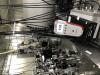
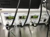
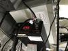
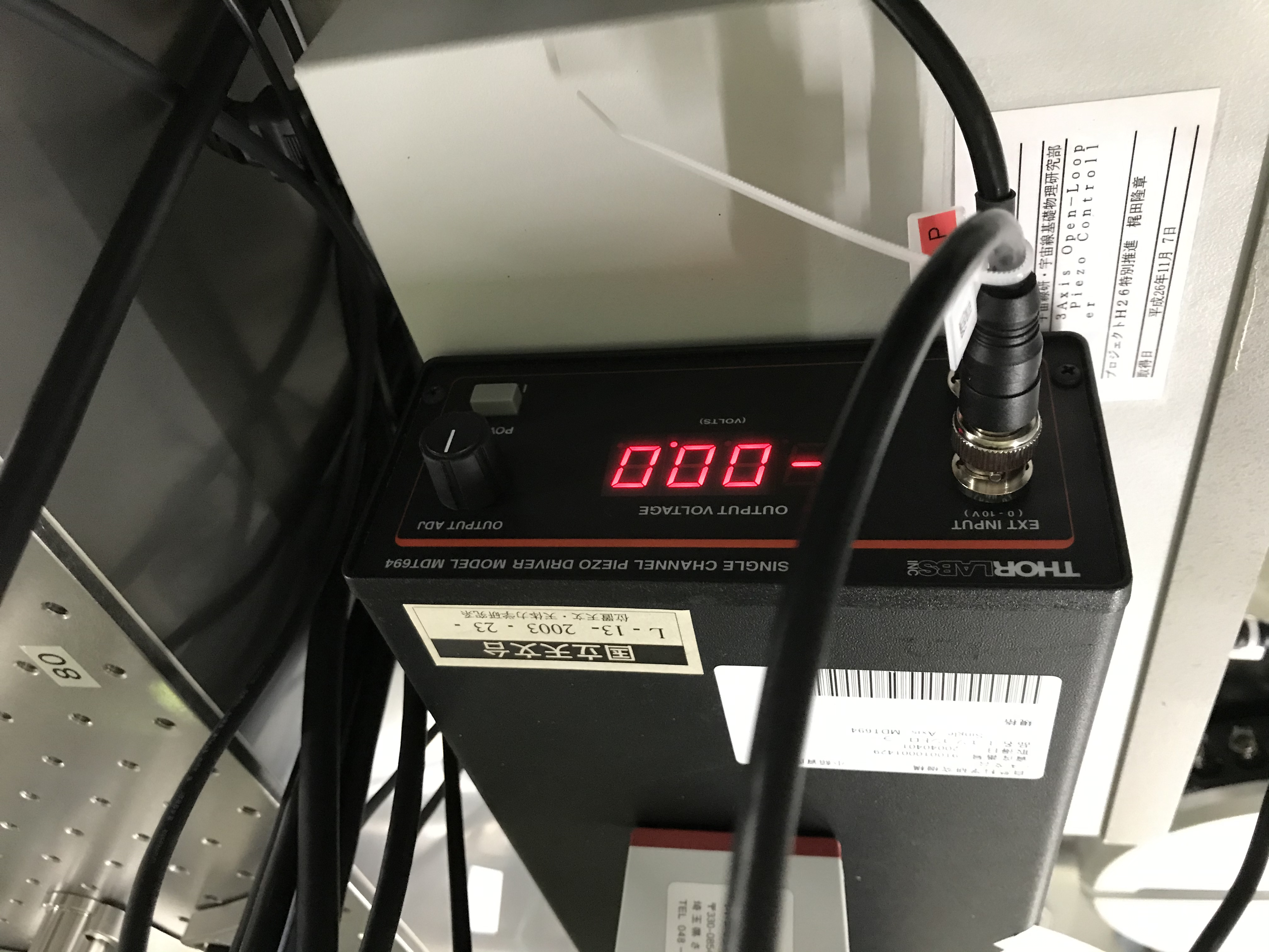
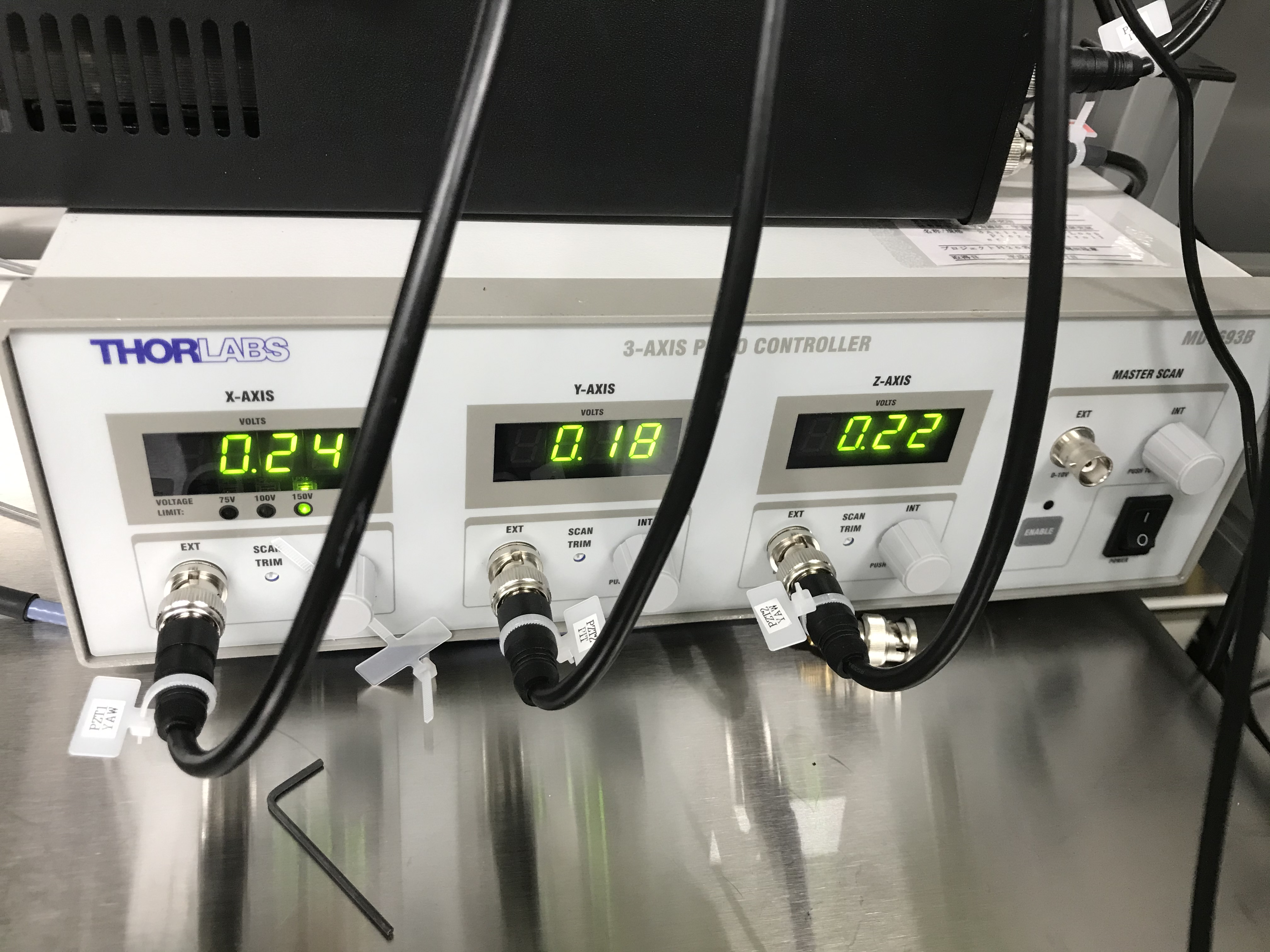
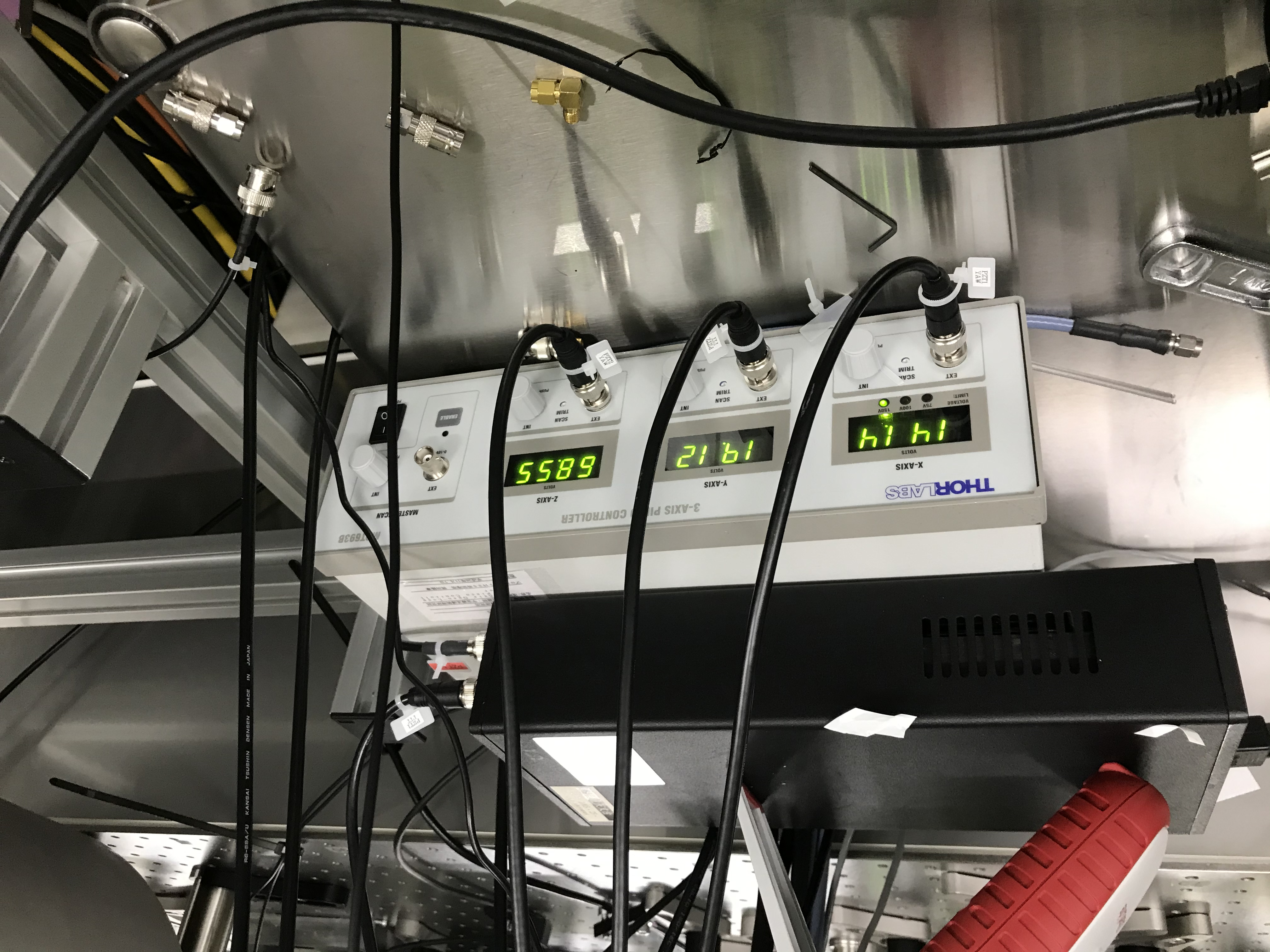
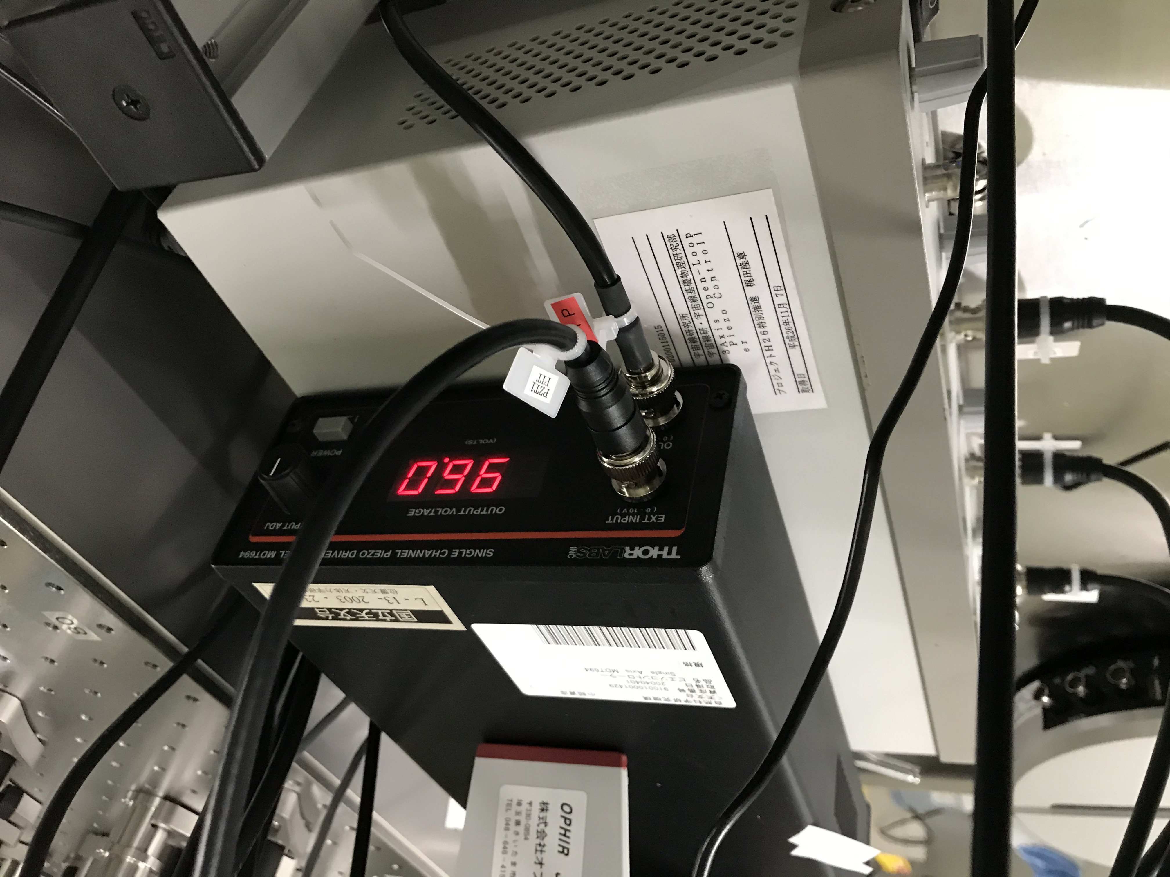
- Ch.5, 6, 7, and 8: provide voltages to PZT drivers. After confirming which BNC voltage output corresponds to which digital system number, we connected the cables, we learned that the offset numbers displayed in the corresponding filter bank (Fig. 8)were just copied at the display of the PZT drivers (these numbers indicate voltages to the PZTs of IPs) (before: Figs. 6 and 7 -> after: Figs. 9 and 10), from which each IP PZT got the driver voltage. By the way, although the PZT driver's range is 0-150V, the provided voltages were near the both edges of the range. We may need to revisit this part later.
- Ch.2: to PMC temperature control: seemed working. let's see. (During the afternoon work, it was saturated. Let's revisit here later.)
- Ch.4: as reported in 16227, as there is a severe concern for the shutter relay driver port, we do not connect this cable; this part will be reported separately later.
By the way, in the past, there was a big campaign to evaluate and reduce the noise due to "ground loop" as reported in 8298 and the jumper pins of the Dsub-to-BNC converter were opened at that time. So maybe we need to do the same evaluation later. I personally estimate that the Ch.4 issue would be one of the principle causes of the large noise. If an opamp is forced to be driven around or over its maximum absolute rating, the opamp shows unexpected behaviors or just broken. I think it might be better to replace the whole circuit of this Dsub-to-BNC converter...
