Reports 1-1 of 1 Clear search Modify search
CRY (Cryo-payload R&D)
dan.chen - 20:09 Tuesday 08 July 2025 (34489) Print this report
Surface figure measurements for sapphire components

With Yoich Aso and Toshihiro Tsuzuki (NAOJ ATC)

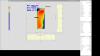
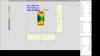
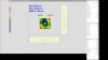
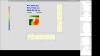
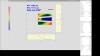
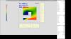
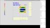
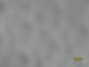
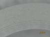
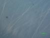
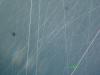
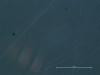
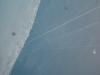
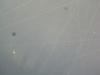
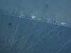
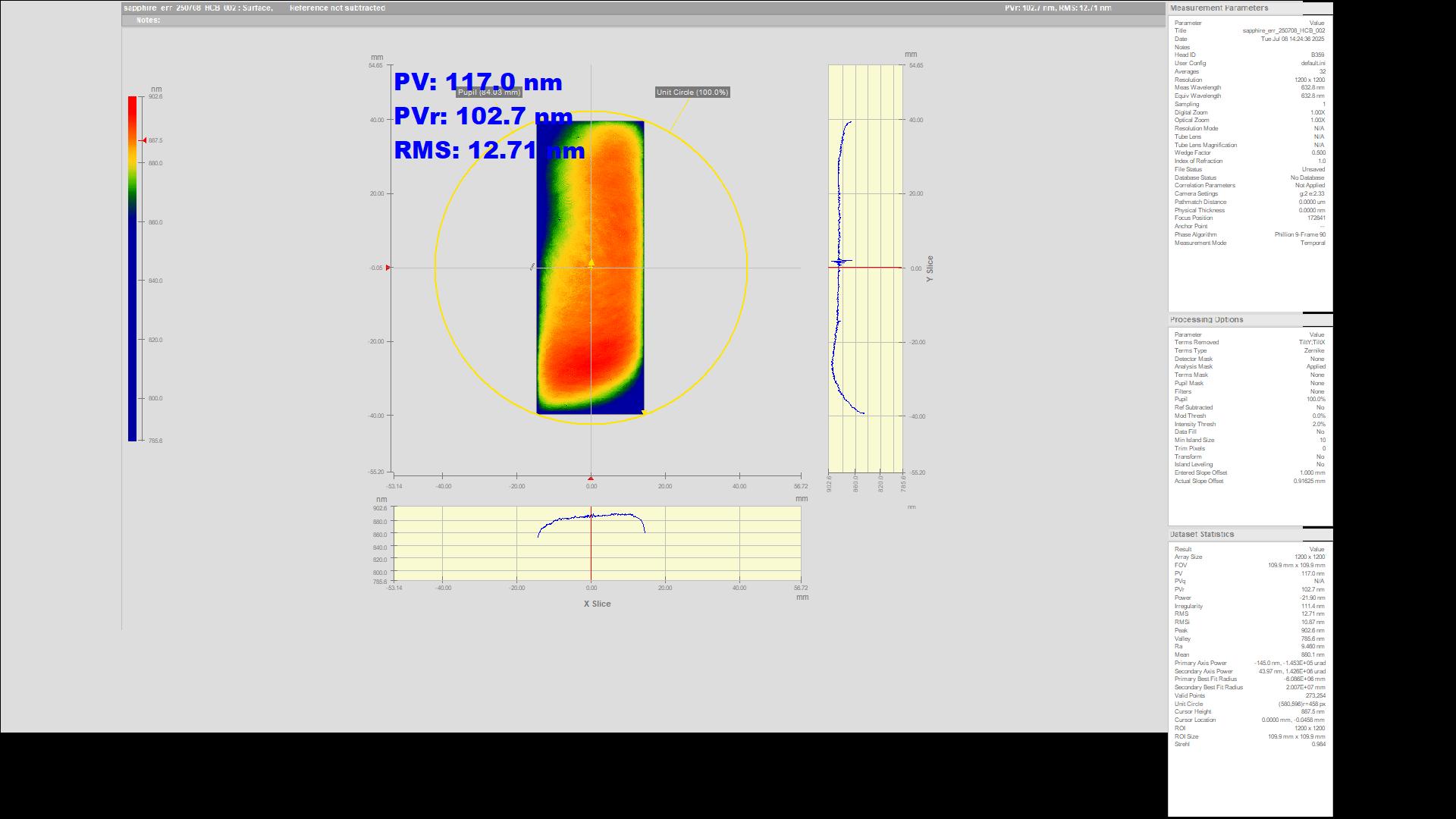
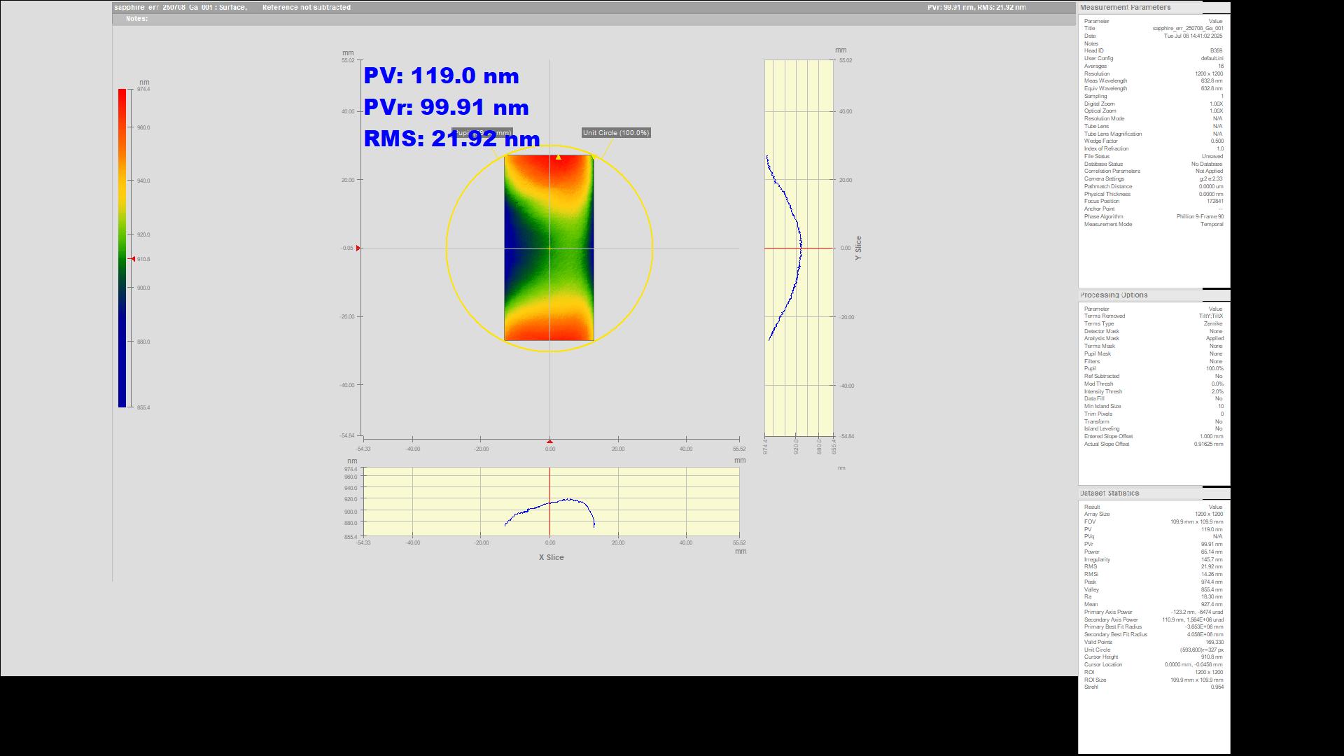
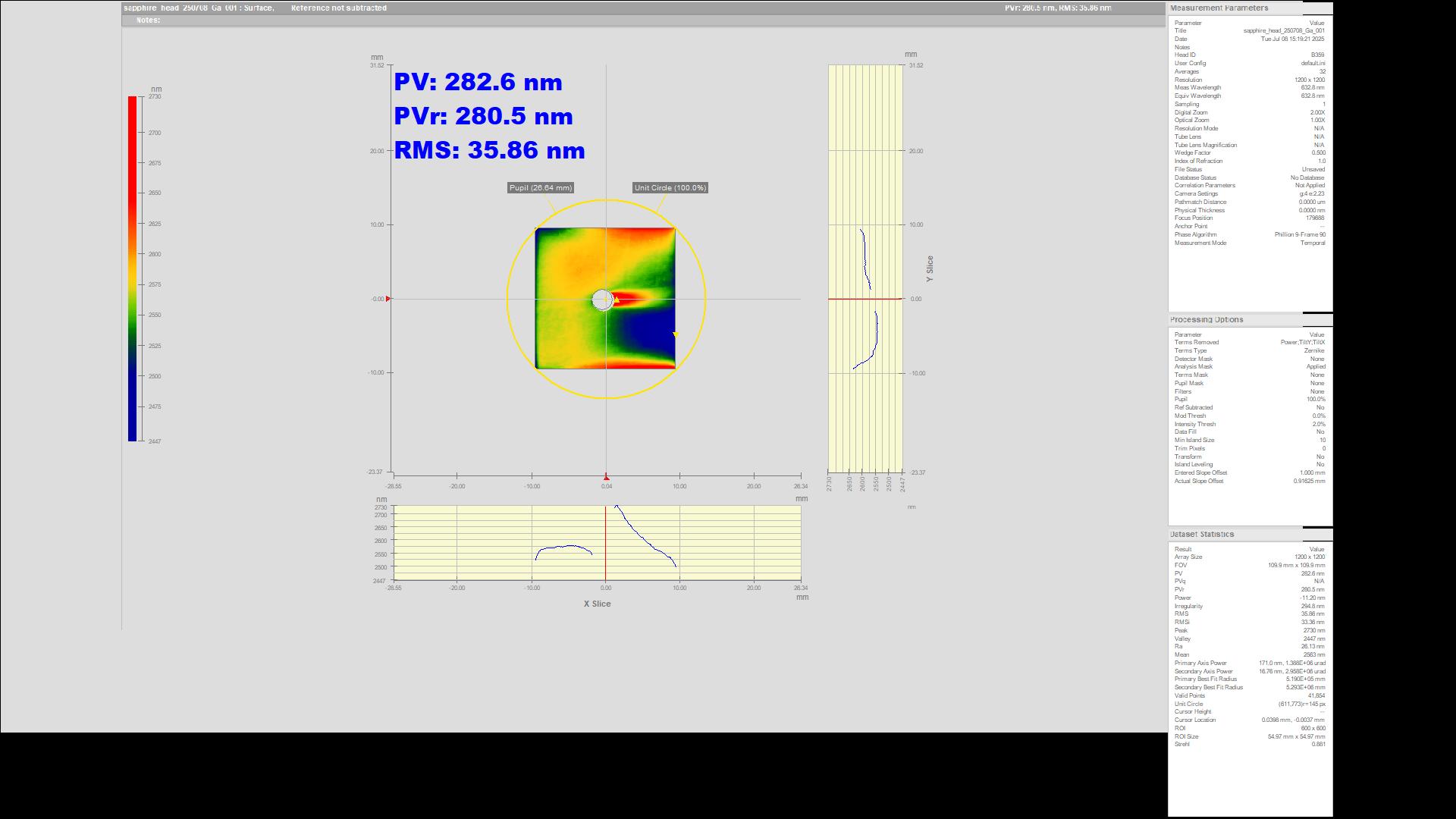
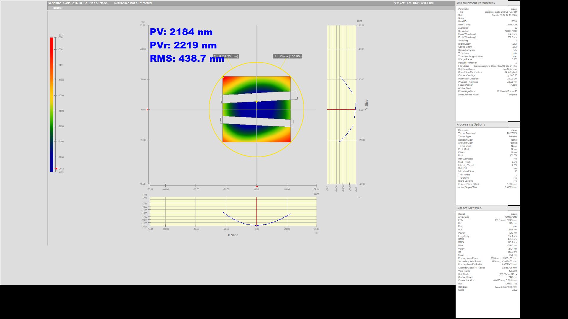
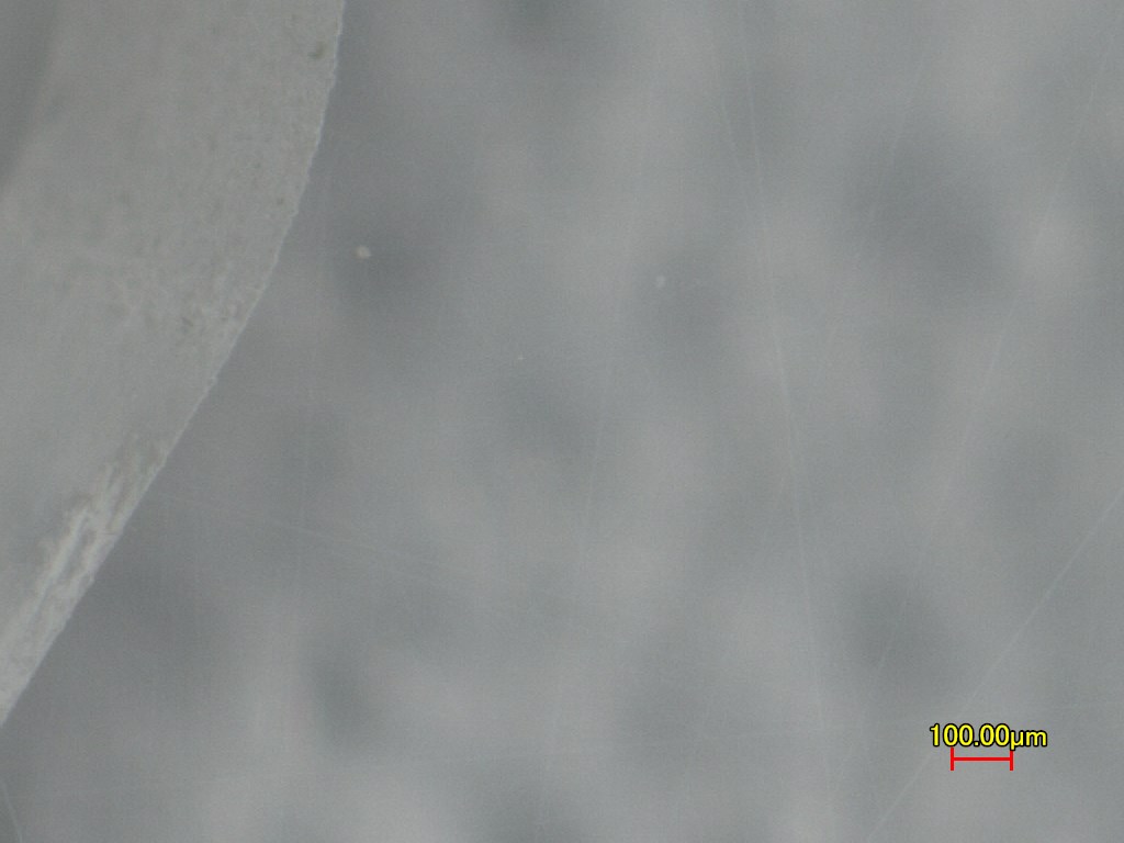
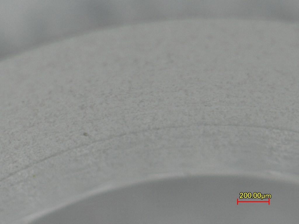
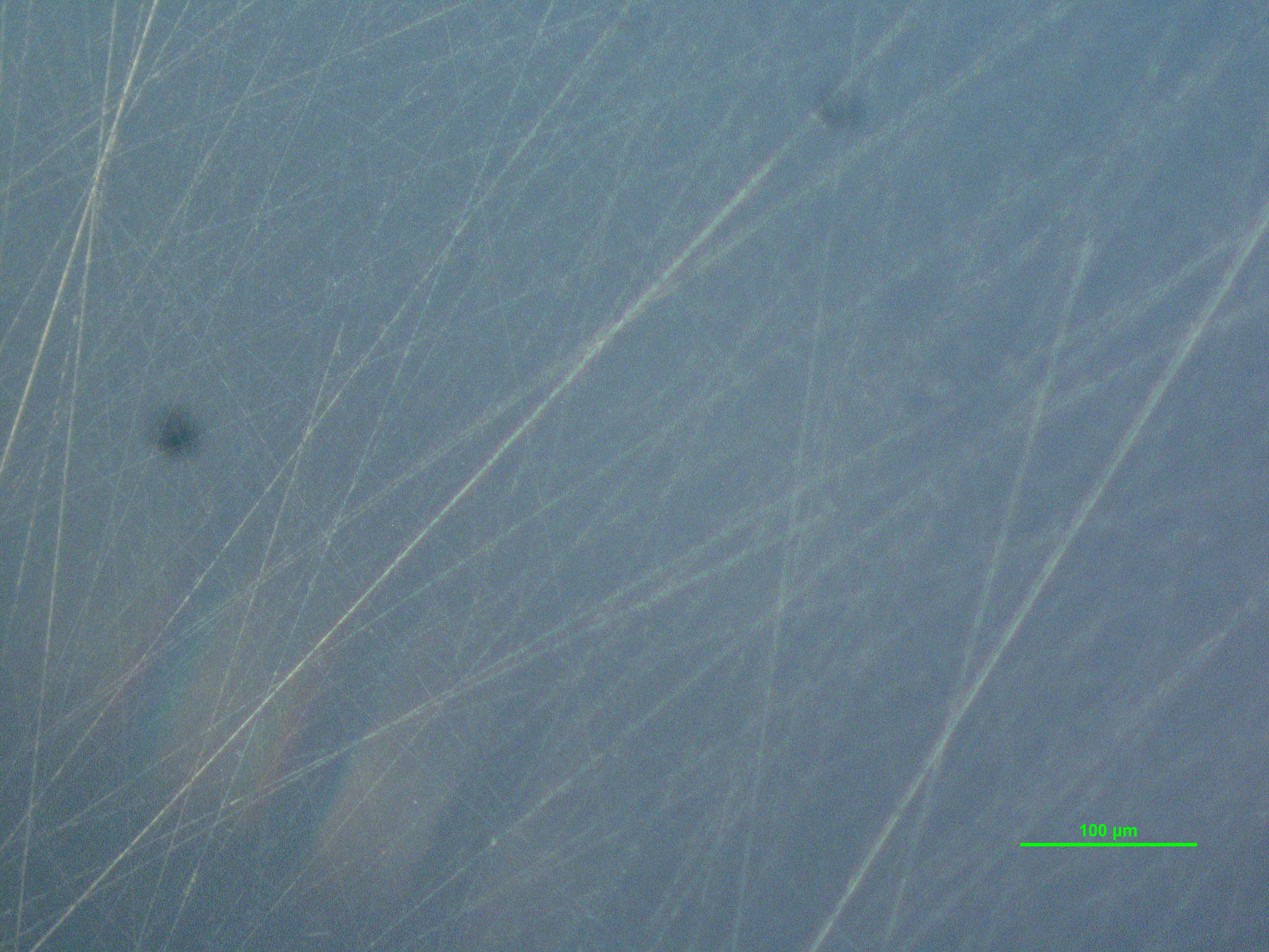
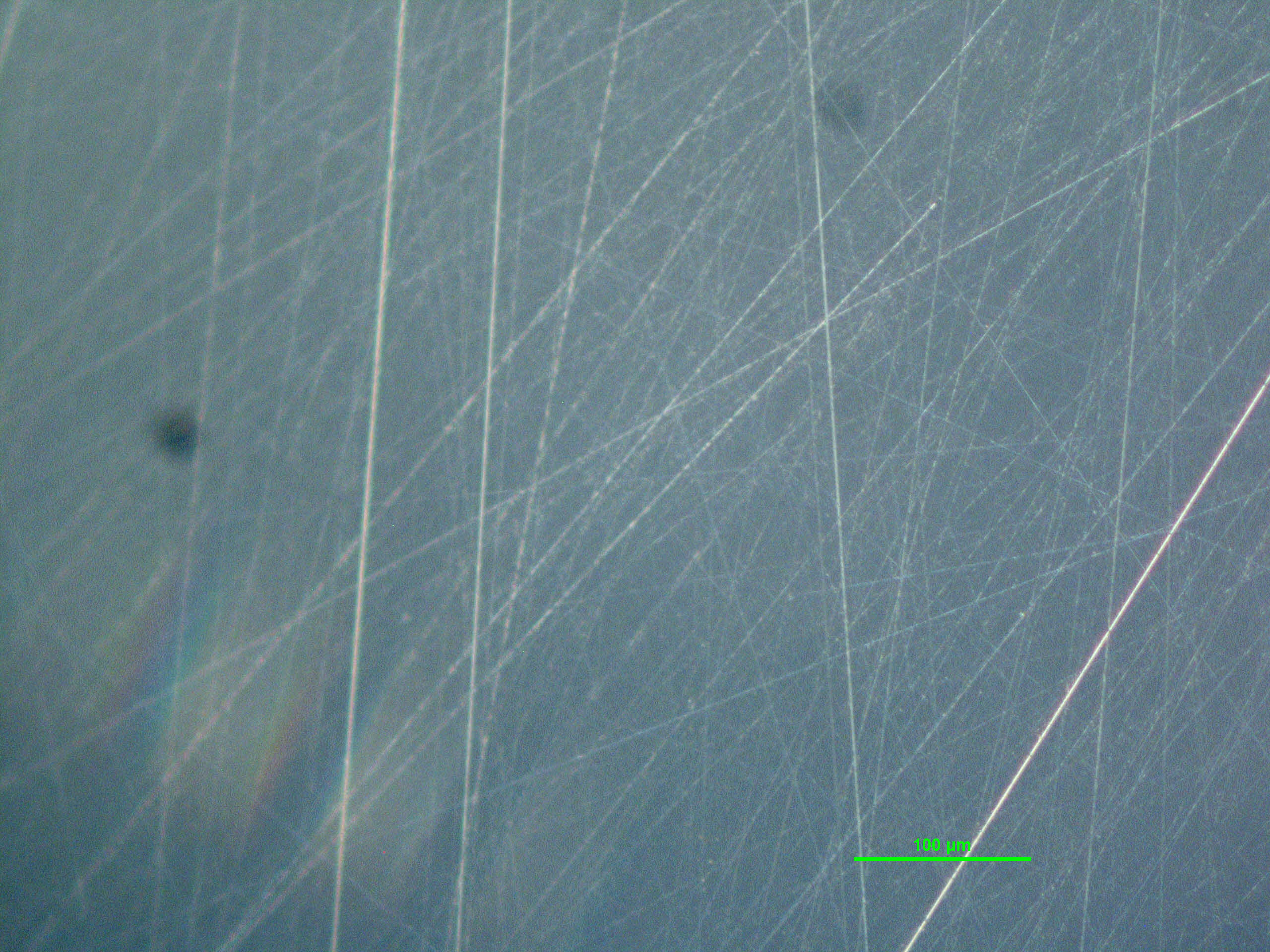
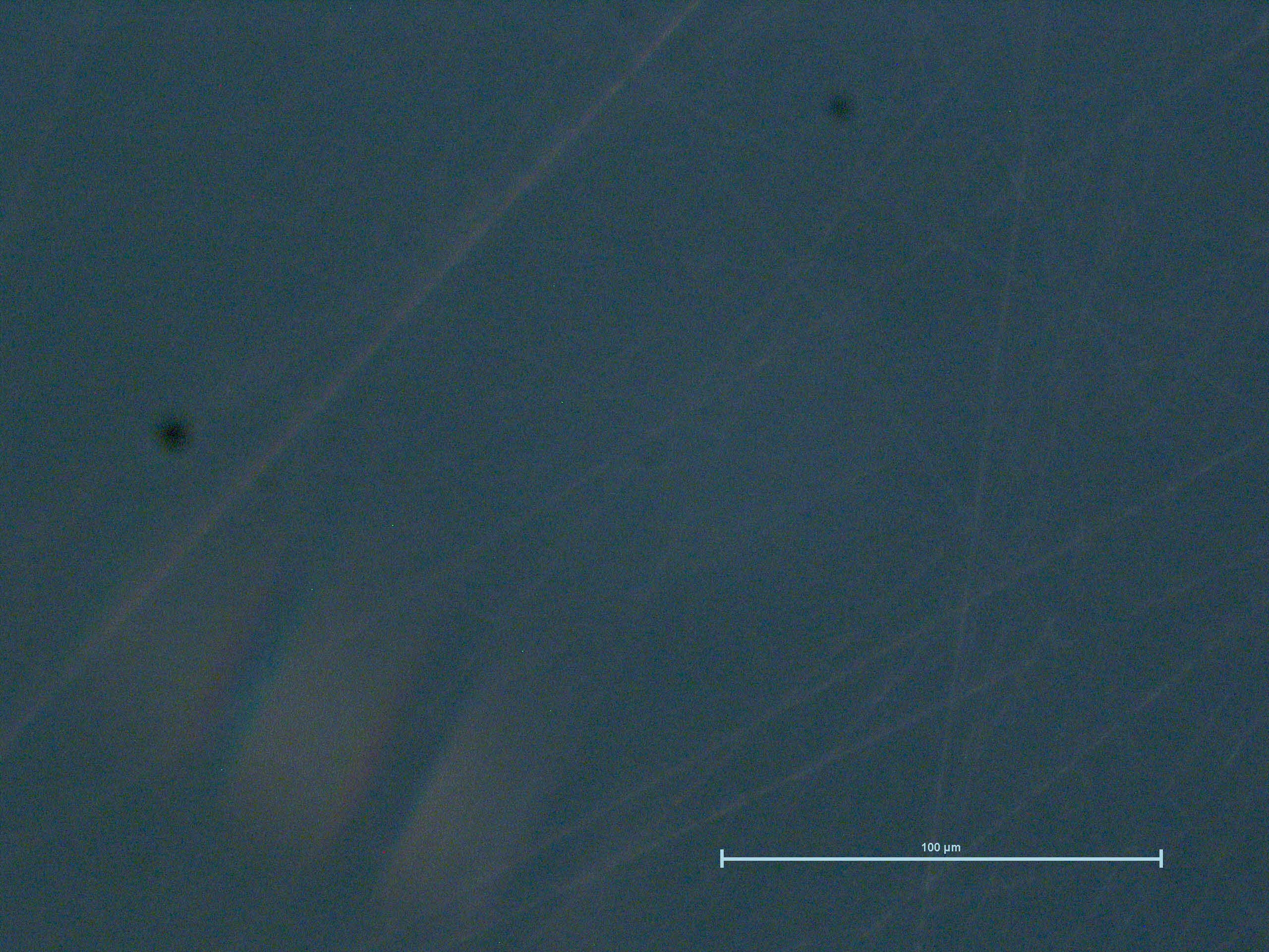
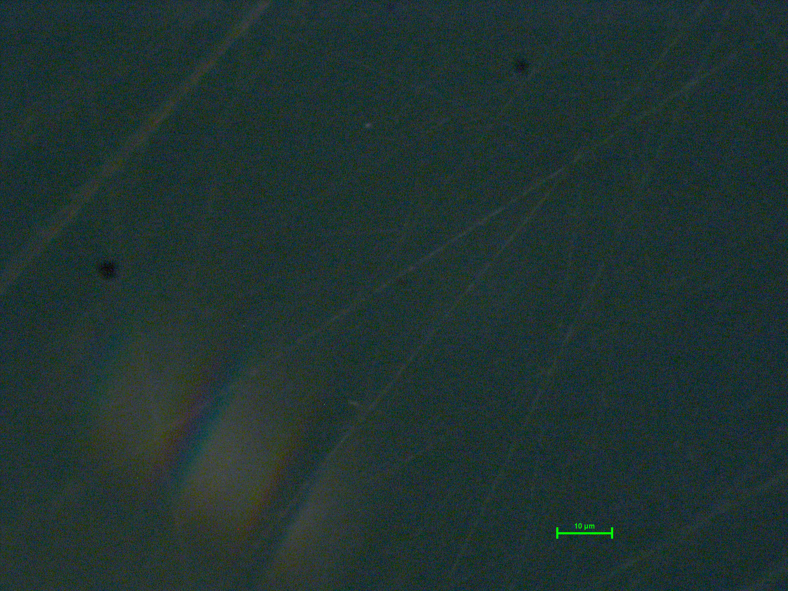
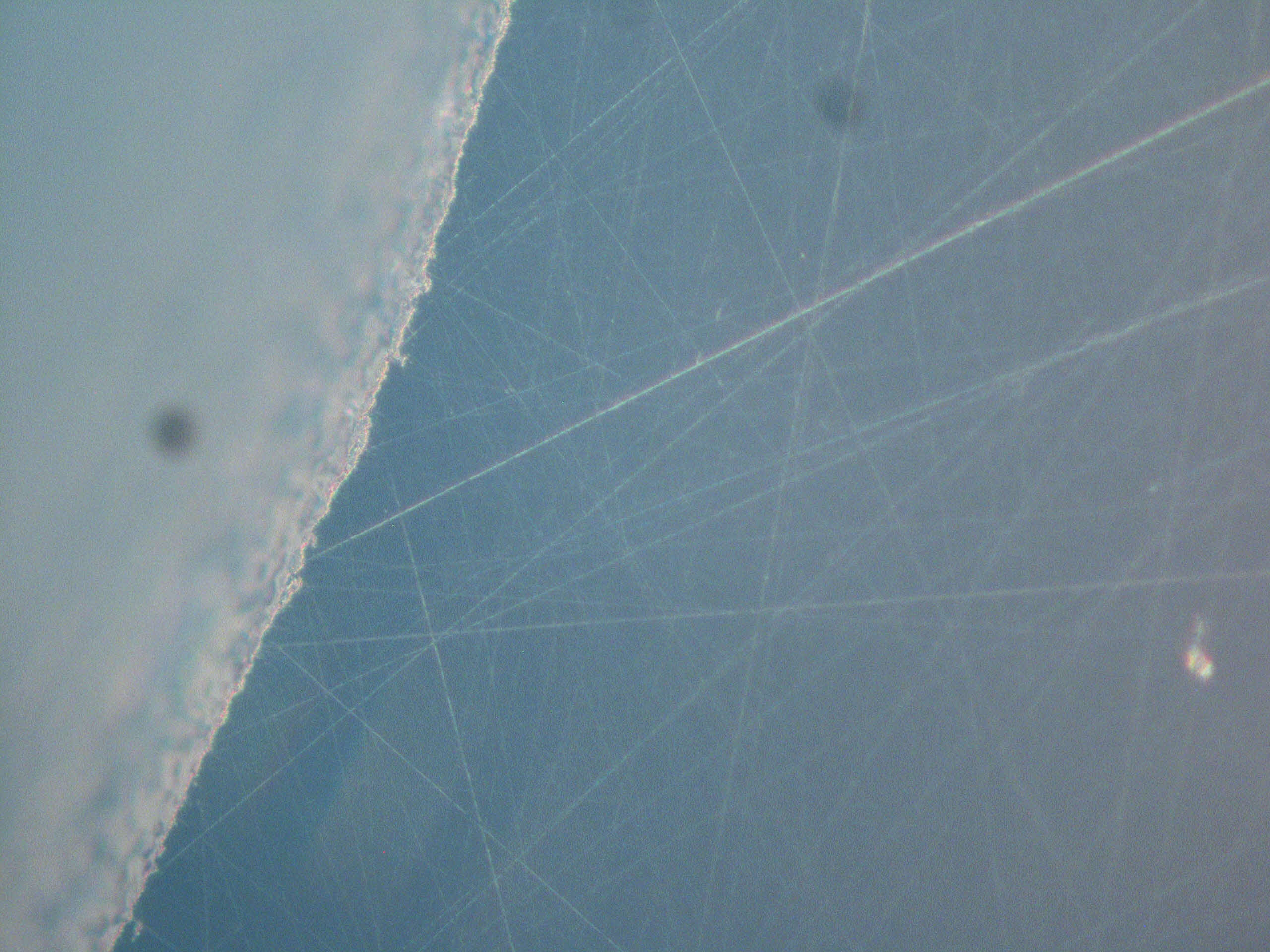
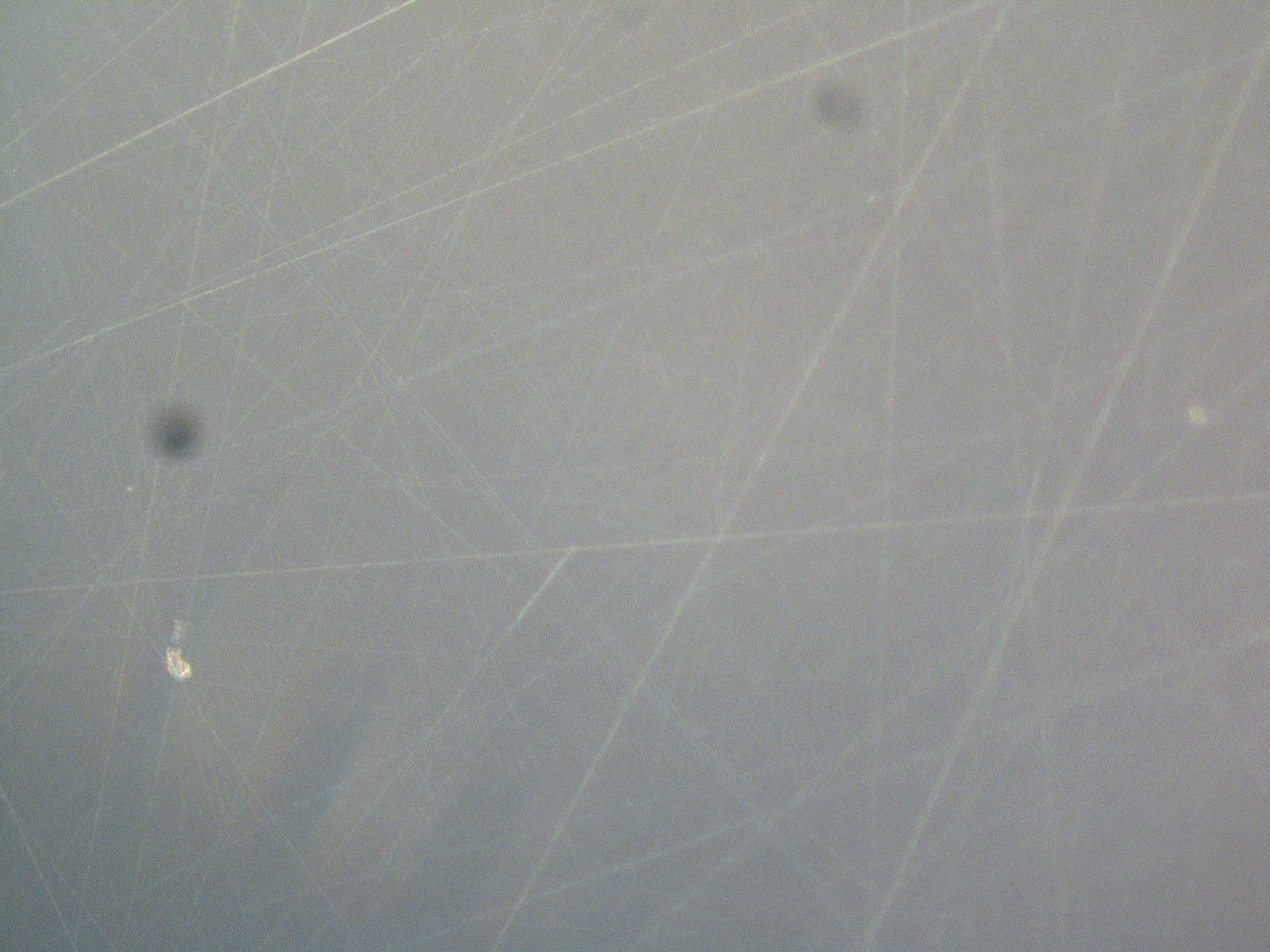
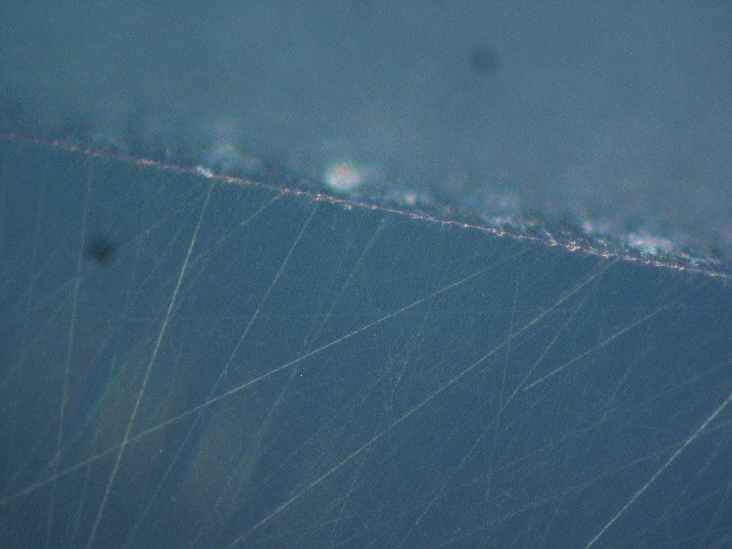
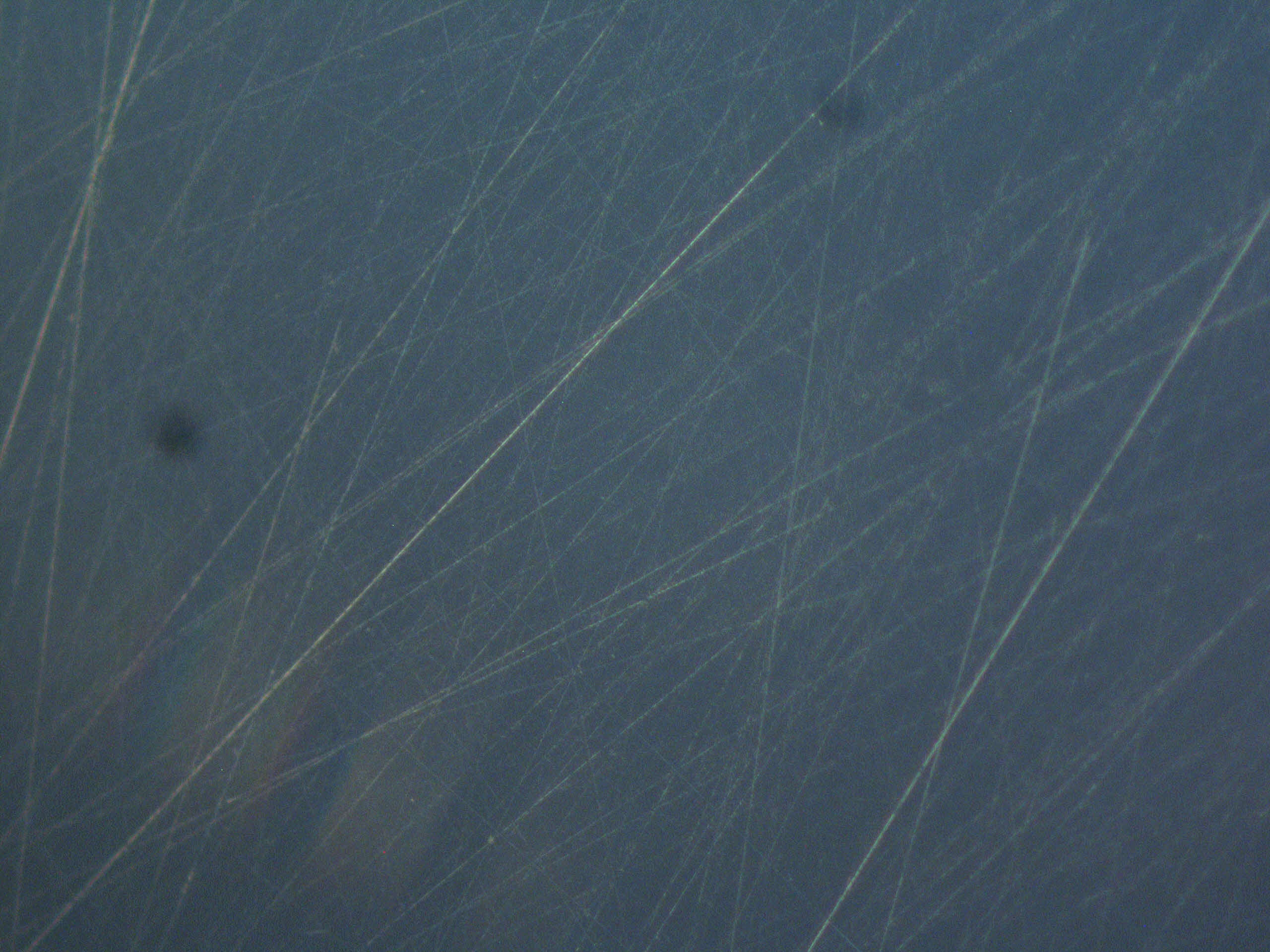
We measured surface figures of a sapphire ear (made by K), a nail head (made by S) and blade spring (made by S).

Measured surface:

  • Sapphire ear
    • Surface for HCB (figure 1, 2: upside down)
    • Surface for Ga bonding (figure 3)
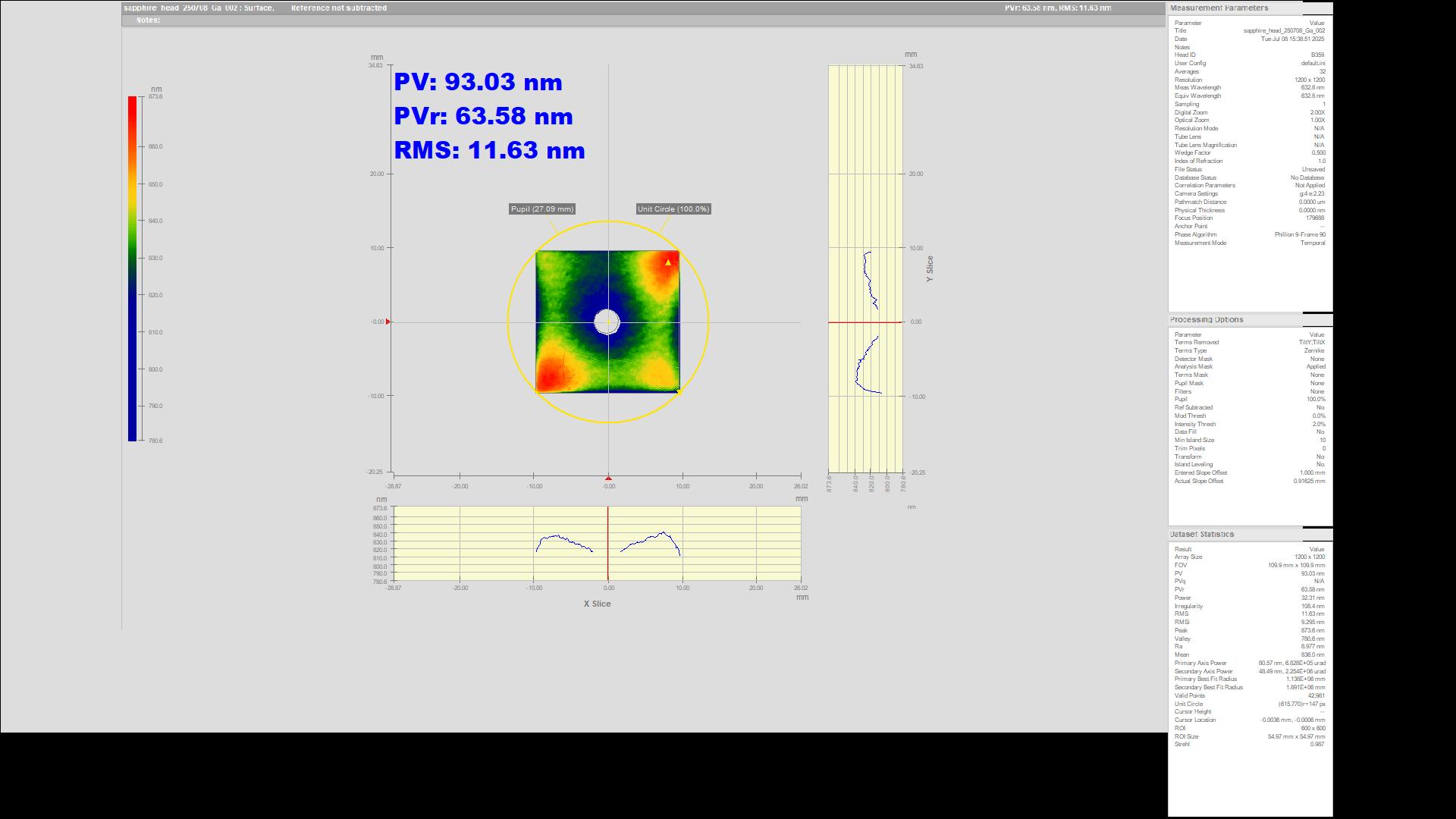
  • Sapphire nail head
    • Surface for Ga (A) (figure 4)
    • Surface for Ga (B) (figure 5)
    • (We can not distinguish A and B)
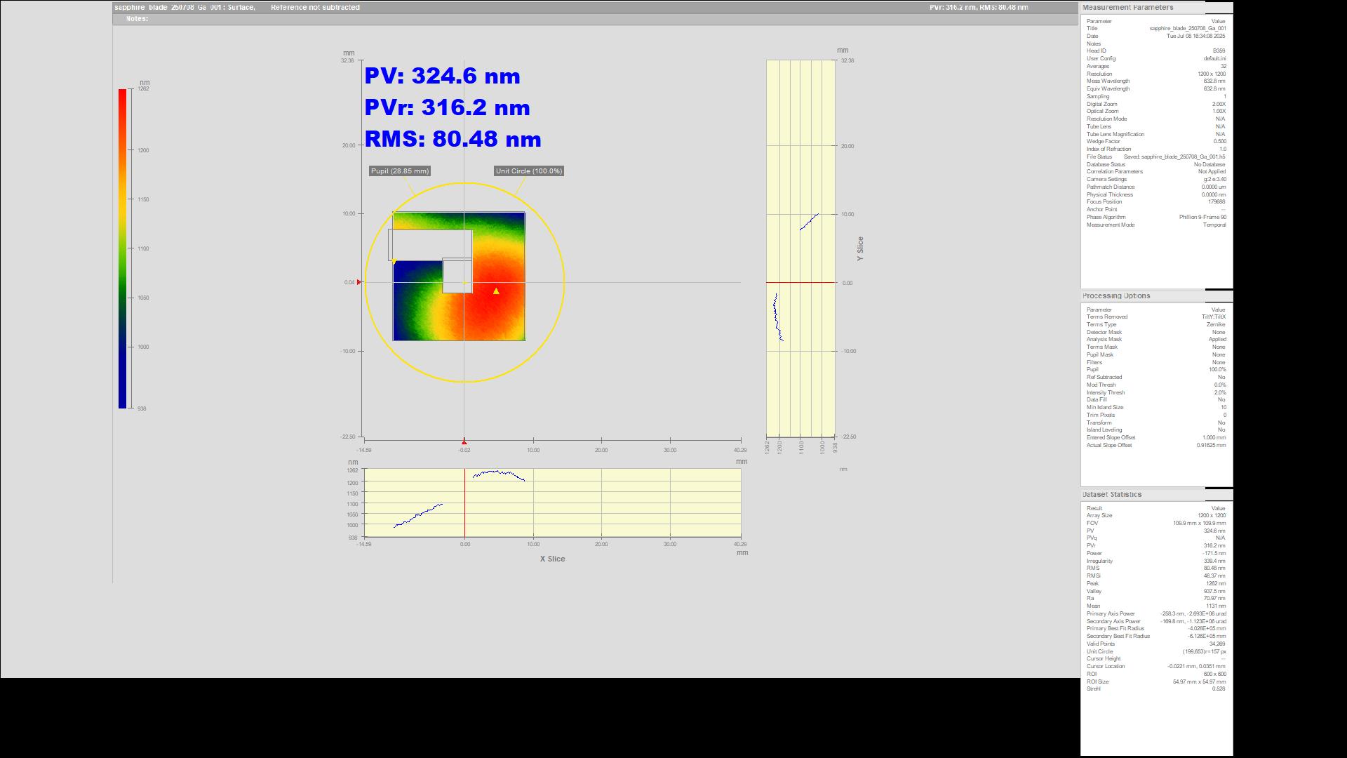
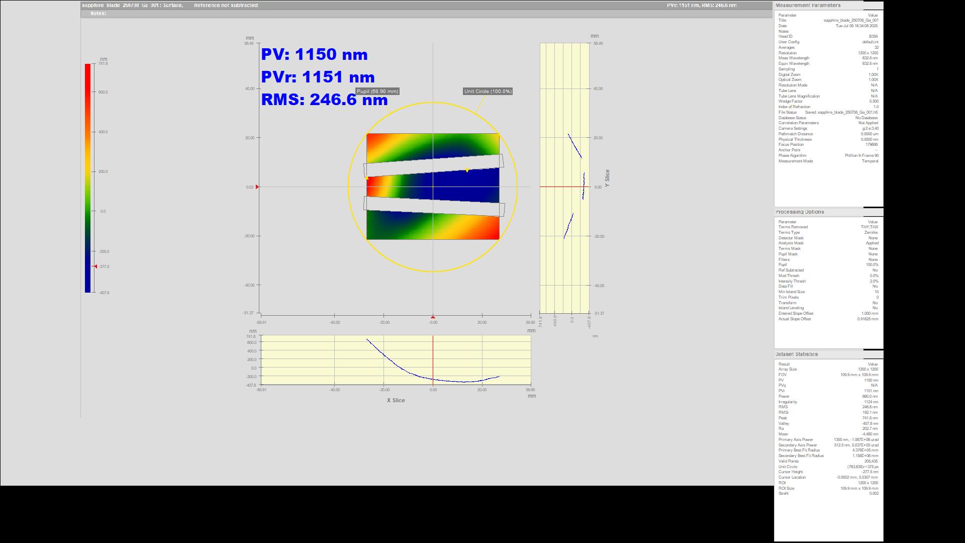
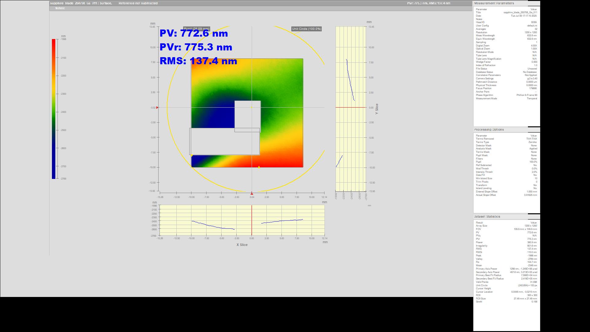
  • Sapphire blade spring
    • Top surface (figure 6,7)
    • Bottom surface (figure 8,9)
    • (We could not distinguish top and bottom at the measurement time.)
    • (Side surfaces could not be measured)

I attached quick results.

Images attached to this report
Comments to this report:
dan.chen - 9:49 Wednesday 09 July 2025 (34491) Print this report

We also used 2 microscopes to have a look on the surface of the blade.

  • Keyence VR3200
  • Nikon NM-40

I attached the pictures taken by the microscopes.

What we saw

  • Numerous linear scratches were observed on the surface. These are clearly visible even to the naked eye.
  • The sloped edges around the hole are noticeably rough.
  • The rim of the hole appears jagged
Images attached to this comment
takafumi.ushiba - 12:56 Wednesday 09 July 2025 (34497) Print this report

Thank you for measuring the surface of sapphire parts.

Is it possible to mask the edge of 1.5mm from the measurement results of HCB surface of sapphire ears?
Our specification of the flatness for HCB surface is 77*27 area of 80*30 surface, so it would be helpful to compare the result with the data from the company.

Search Help
×

Warning

×