With Terrence
In case you don't see the picture attached to this report, please click this link: 9658.
After the LVDT driver broke down on the 24th of July (entry 9659) we replaced it by a new one. In order to keep the same LVDT calibration factors for each channel we adjusted the values of
- One input gain resistor (see text below),
- One output gain resisitor (see entry 9025) and
- One phase determined by a resisitance value (see entry 9025).
According to Joris's and Enzo's documents (JGW-T1604798 and JGW-E1707287 respectively), the input gains (whose values were reported in entry 9025) are adjusted by changing the values of the variable resistors shown in the picture and the effect can be seen in the amplitude of the signal measured between ground and probe points P0, P1, P2 and P3 for each channel respectively. However, when we tried varying the amplitudes we didn't see any obvious change on the oscilloscope screen. Because the resistors are not labeled on the PCB board we even adjusted the four of them for one single signal but we didn't see any obvious change.
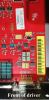
The alternative strategy was then to measure the values of the resistors in the broken LVDT driver cards and adjust the new driver accordingly. The resistors are labeled A, B, C and D as shown in the first picture. The values were measured between the resistors' accesible terminals and probe point P_resistor (see picture), which is terminal 2 of the OPA211 (see sheet 2 of the circuit diagram: JGW-D1301467-v1). The measured values are given according to the position of the board (as seen from the front) and the position of the resistor:
- Left A: 5.811 kΩ
- Left B: 3.750 kΩ,
- Left C: 1.364 kΩ,
- Left D: 5.187 kΩ,
- Right A: 5.466 kΩ,
- Right B: 5.408 kΩ,
- Right C: 5.619 kΩ,
- Right D: 5.498 kΩ.
Therefore, the settings of the boards are given by the table in entry 9025 with the resistance values given here replacing the input gain values in the table.