Abstract
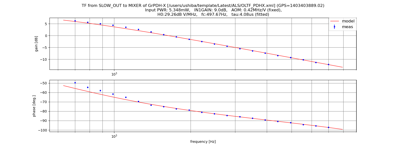
I tried to estimate the optical gain of GrPDH-X by using measured OLTF in klog#30125 and AOM efficiency measured in klog#6544.
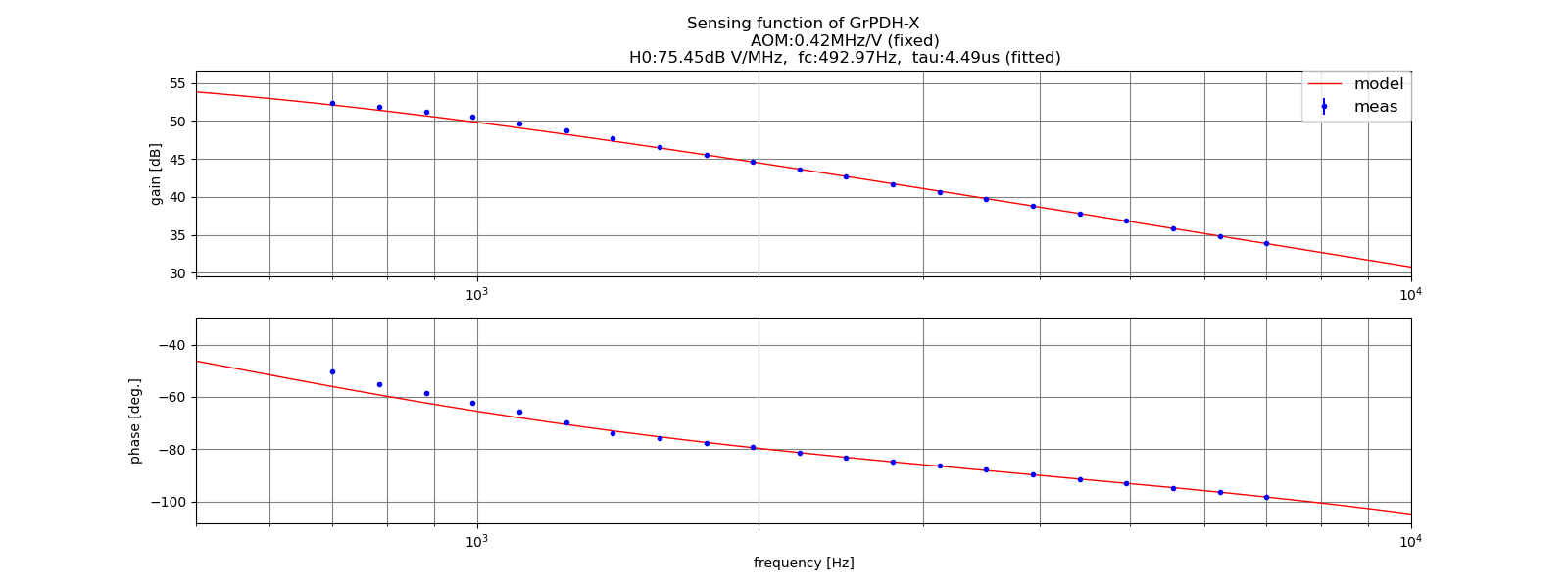
Best fitted value of optical gain and cavity pole frequency is 75.45dB V/MHz and 492.97Hz, respectively (expected rough cavity pole frequency is ~500Hz).
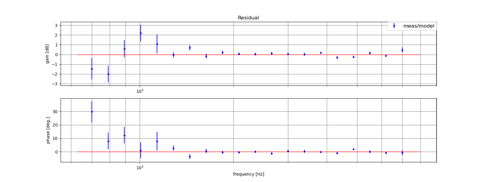
Individual difference at generic filter for SLOW_DAQ may make a mismatch as ~0.6dB, 6deg. around 1kHz because I assumed it as design value.
Measuring generic filter response and modeling it might be able to remove this remaining mismatch (though I don't think it's not urgent).
Details
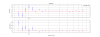
Measured transfer function by Ushiba-kun is from K1:ALS-X_PDH_SLOW_DAQ_OUT_DQ to K1:ALS-X_PDH_MIXER_DAQ_OUT_DQ. K1:ALS-X_PDH_SLOW_DAQ_OUT_DQ is calibrated to the single-end voltage at the input point of slow lowpass. ALS-X_PDH_MIXER_DAQ_OUT_DQ is calibrated to the single-end voltage at the input point of common compensation. These two calibrations are applied at the FilterBank modules. In addition to this, Ushiba-kun applied the analog filter responses of CMS to his measurement results by diaggui calibration in order to obtain the transfer function corresponding to OLTF. For my purpose, simulating analog filter response of CMS is not required and difference between design value and actual electronics may affect estimated optical gain. So I used raw transfer function from K1:ALS-X_PDH_SLOW_DAQ_OUT_DQ to K1:ALS-X_PDH_MIXER_DAQ_OUT_DQ without diaggui calibration in my estimation.
This raw transfer function should contain following components.
- slow lowpass filter: 500kHz LPF ["List of variants" in Wiki page]
- AOM efficiency: 0.42MHz/V [klog#6544]
- optical response (optical gain + cavity pole)
- mini-circuit attenuator and lowpass at IN1 of CMS: -20dB and 1.6MHz LPF [JGW-T2112593]
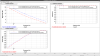
- IN1GAIN of CMS: 9dB [Fig.1 (IN1GAIN value at the measurement time)]
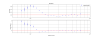
I fitted the measured raw transfer function with the model function containing these components. In this fitting only optical gain and cavity pole frequency are treated as the free parameters and other components were fixed the designed value. And also, Because I could see phase delay by super-Nyquist pole or the time delay around Nyquist frequency, I added the time delay parameter as exp(-i*2*pi*f*tau).
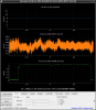
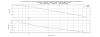
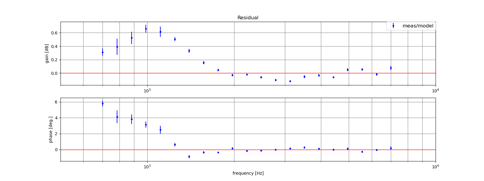
Fitted results are shown in Fig.2 and Fig.3. Best fitted value of optical gain, cavity pole frequency and empirical time delay is 75.45dB V/MHz, 492.97Hz, and 4.49us, respectively. Note that optical gain means a conversion factor from voltage at the input of mini-circuits on IN1 port of CMS to frequency. Though this is a fitting with very simple single pole model, correlation between fitting parameters are not so small because all measured data points are larger than the pole frequency. But estimated cavity pole frequency is roughly same as expected value. So these best fitted value seems to be not so bad estimation.
According to the residual plot (Fig.3), there is frequency dependent structure. Because this structure is only ~0.6dB, it seems to come from a mismatch in zero/pole frequency or a poor SNR of the excitation signal instead of the missing zero/pole. So model function itself is not so bad. This estimation is not affected by the individual differences of compensation and boost filters in common/slow paths. So possible case of the mismatch in zero/pole frequency is generic filter at MIXER_DAQ or SLOW_DAQ.